This article is a continuation of the series of tutorials on the LPC2148 Microcontroller (ARM7). The aim of this series is to provide easy and practical examples that anyone can understand. In the previous tutorial, we have seen how to create a project in Keil for LPC2148 (ARM7). Now we will see LPC2148 PLL (Phase Locked Loop) Tutorial. PLL stands for Phase-Locked Loop and is used to generate clock pulse given a reference clock input which is generally from a crystal oscillator(or XTAL). Configuring and using PLL in lpc124x MCUs is pretty simple and straightforward.
Table of Contents
Suggestion to read
Introduction
There are several ways we can clock ARM Microcontroller. One way is to use External Clock with duty cycle 50-50 and in a frequency range 1 MHz to 50 MHz connected to XTAL1 Pin. The second way is by connecting External Crystal Oscillator but its range is lower between 1 MHz to 30 MHz. We can also use on-chip PLL Oscillator but here external clock frequency should not exceed range from 10 MHz to 25 MHz. In this tutorial, we will concentrate on External Crystal with PLL.
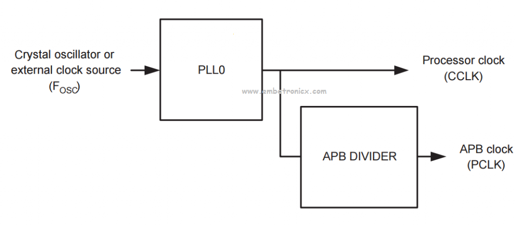
In this tutorial, we will focus only on PLL0 as it is the main clock signal which acts as the CPU clock and also goes to on-chip peripherals.
LPC2148 PLL (Phase Locked Loop) Tutorial
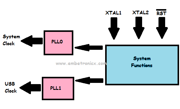
There are two PLL modules in the LPC2141/2/4/6/8 microcontroller. The PLL0 is used to generate the CCLK clock (system clock) while the PLL1 has to supply the clock for the USB at the fixed rate of 48 MHz. Structurally these two PLLs are identical with exception of the PLL interrupt capabilities reserved only for the PLL0.
The PLL0 and PLL1 accept an input clock frequency in the range of 10 MHz to 25 MHz only. The input frequency is multiplied up the range of 10 MHz to 60 MHz for the CCLK and 48 MHz for the USB clock using a Current Controlled Oscillators (CCO). The multiplier can be an integer value from 1 to 32 (in practice, the multiplier value cannot be higher than 6 on the LPC2141/2/4/6/8 due to the upper frequency limit of the CPU).
ARM7 LPC2148 Microcontroller needs two clocks; one is for its peripherals and the other for its CPU. CPU works faster with higher frequencies whereas peripheral needs lower frequency to work with. The Peripheral Clock (PCLK) and CPU Clock (CCLK) gets clock input from a PLL or from external source. After RESET, the configuration of PLL (Phase Lock Loop) and VPB (VLSI Peripheral Bus) Divider would be the first thing to do.
PLL unit itself uses CCO (Current Controlled Oscillator) which operates in the range between 156 MHz to 320 MHz, so there is additional divider which keeps CCO within its range, while PLL provides desired frequency. The output clock is generated by dividing CCO frequency by 2, 4, 8, 16. Minimum divider is ‘2’ so output of PLL will always have duty cycle 50% for sure.
The Peripheral Clock i.e. PCLK is derived from CPU Clock i.e. CCLK. The APB Divider decides the operating frequency of PCLK. The input to APB Divider is CCLK and output is PCLK. By Default, PCLK runs at 1/4th the speed of CCLK. To control APB Divider we have a register called VPBDIV. The value in VPBDIV controls the division of CCLK to generate PCLK as shown below:
The following table shows the possible values of VPBDIV and the corresponding PCLK values.
| VPBDIV = 0x00 | PCLK is ¼ of CCLK |
| VPBDIV = 0x01 | PCLK is equal to CCLK |
| VPBDIV = 0x02 | PCLK is ½ of CCLK |
| VPBDIV = 0x03 | Reserved. No effect. |
Associate Registers for PLL – LPC2148 PLL (Phase Locked Loop) Tutorial
-
PLLCON (PLL Control Register)
-
PLLCFG (PLL Configuration Register)
-
PLLSTAT (PLL Status Register)
-
PLLFEED
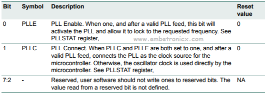
PLLCON (PLL Control Register)
The PLLCON register contains the bits that enable and connect the PLL. Enabling the PLL allows it to attempt to lock to the current settings of the multiplier and divider values. Connecting the PLL causes the processor and all chip functions to run from the PLL output clock. Values written to this register do not take effect until a valid PLL feed sequence has taken place.
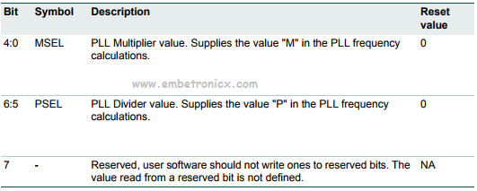
PLLCFG (PLL Configuration Register)
The PLLCFG register contains the PLL multiplier and divider values. Values written to this register do not take effect until a valid PLL feed sequence has taken place.
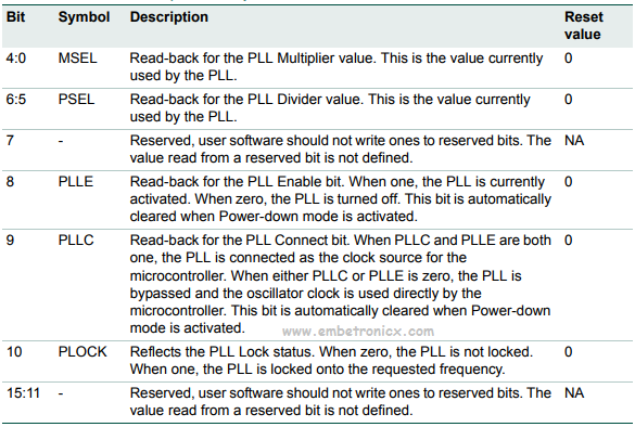
PLLSTAT (PLL Status Register)
Read-back register for PLL control and configuration information. If PLLCON or PLLCFG have been written to, but a PLL feed sequence has not yet occurred, they will not reflect the current PLL state. Reading this register provides the actual values controlling the PLL, as well as the status of the PLL.
PLLFEED (PLL Feed Register)
A correct feed sequence must be written to the PLLFEED register in order for changes to the PLLCON and PLLCFG registers to take effect. The feed sequence is:
-
Write the value 0xAA to PLLFEED.
-
Write the value 0x55 to PLLFEED.
The two writes must be in the correct sequence, and must be consecutive APB bus cycles. The latter requirement implies that interrupts must be disabled for the duration of the PLL feed operation. If either of the feed values is incorrect, or one of the previously mentioned conditions is not met, any changes to the PLLCON or PLLCFG register will not become effective.
PLL frequency calculation
Let’s define some symbols which are used in Datasheet and also which I’ll be using in this tutorial :
- FOSC => frequency from the crystal oscillator(XTAL)/external clock
- FCCO => frequency of the PLL Current Controlled Oscillator(CCO)
- CCLK => PLL output frequency (CPU Clock)
- M => PLL Multiplier value from the MSEL bits in the PLLCFG register
- P => PLL Divider value from the PSEL bits in the PLLCFG register
- PCLK => Peripheral Clock which is derived from CCLK
Now, the PLL output clock is given by the formula:
CCLK = M x FOSC
or
CCLK = FCCO / (2 x P)
CCO output clock is given by:
FCCO = CCLK x 2 x P
or
FCCO = FOSC x M x 2 x P
Note:
The PLL inputs and settings must meet the following:
-
FOSC is in the range of 10 MHz to 25 MHz.
-
CCLK is in the range of 10 MHz to Fmax(the maximum allowed frequency for the microcontroller – determined by the system microcontroller is embedded in).
-
FCCO is in the range of 156 MHz to 320 MHz.
Setting Up PLL – LPC2148 PLL (Phase Locked Loop) Tutorial
Explaining the internal working of PLLs and CCOs in detail is not in the scope of this tutorial. Here we are just concerned about its usage rather than knowing its internals.
The Order of setting up PLLs is strict as follows :
-
Setup PLL
-
Apply Feed Sequence
-
Wait for PLL to lock and then Connect PLL
-
Apply Feed Sequence
Setup PLL
-
Choose the desired processor operating frequency (CCLK). This may be based on processor throughput requirements, need to support a specific set of UART baud rates, etc. Bear in mind that peripheral devices may be running from a lower clock than the processor.
-
Choose an oscillator frequency (FOSC). CCLK must be the whole (non-fractional) multiple of FOSC.
-
Calculate the value of M to configure the MSEL bits. M = CCLK / FOSC. M must be in the range of 1 to 32. The value written to the MSEL bits in PLLCFG is M 1.
-
Find a value for P to configure the PSEL bits, such that FCCO is within its defined frequency limits. F CCO is calculated using the equation given above. P must have one of the values 1, 2, 4, or 8. The value written to the PSEL bits in PLLCFG is 00 for P = 1; 01 for P = 2; 10 for P = 4; 11 for P = 8
Let us assume that the CPU frequency is at the maximum possible value i.e. 60 MHz. We will calculate the values of P and M with this frequency in mind.
Values of PSEL for P are :

Now, Since there is no point in running the MCU at lower speeds than 60Mhz (except in some situations) ill put a table giving values for M and P for different crystal frequencies i.e FOSC.
Since CCLK = 60 MHz, we can calculate the value of P as follows. The equation to calculate P is given by
P = FCCO / (2 X CCLK)
We know that the range of FCCO is 156 MHz to 320 MHz.
Substituting FCCO = 156 MHz, we get P = 156 MHz / (2 X 60 MHz) = 1.3.
Substituting FCCO = 320 MHz, we get P = 320 MHz / (2 X 60 MHz) = 2.67.
Since the value of ‘P’ must be an integer, the integer between 1.3 and 2.6 is ‘2’.
As we got the value of ‘P’ as ‘2’, the value in the PSEL bits should be ‘01’.
We will now calculate the value of ‘M’. From the above mentioned formulae, we can calculate the value of ‘M’ using the following formula.
M = CCLK / FOSC
The following table indicates a list of possible crystal oscillator values along with the values of ‘M’, ‘MSEL’, ‘P’, ‘PSEL’ and the value in the PLL0CFG register.
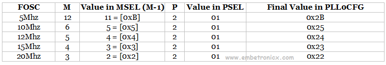
Note: 12 MHz is the most common value for crystal oscillator in many microcontroller development boards. If the development you are using has a different crystal oscillator (for some strange reason), then we need to consider the values of ‘M’ and ‘P’.
PLL0CON=0x01; // PPLE=1 & PPLC=0 so it will be enabled  but not connected after FEED sequence
PLL0CFG=0x24;  // set the multipler to 5 (i.e actually 4) i.e 12x5 = 60 Mhz (M - 1 = 4), Set P=2 since we want FCCO in range So , Assign PSEL =01 in PLL0CFG as per the table.
Apply Feed Sequence
Feed Sequence is nothing but assignment of 2 particular ‘fixed’ values to a register related to the PLL block. This register is called ‘PLL0FEED’. And those fixed values are 0xAA and 0x55 are in order!. Hence the code for feed sequence must be :
PLL0FEED=0XAA;					//feed
PLL0FEED=0X55;
Wait for PLL to lock and then Connect PLL
Check whether PLL has locked on to the desired freq by reading the lock bit in PLL0STST register. If it locked then connect the PLL by setting the 2nd bit in PLL0CON Register.
while((PLL0STAT&(1<<10))==0); // check whether PLL has locked on to the  desired freq by reading the lock bit in the PPL0STAT register
PLL0CON=0x03;			     //enable & connect pll
Apply Feed Sequence
Feed Sequence is nothing but assignment of 2 particular ‘fixed’ values to a register related to the PLL block. This register is called ‘PLL0FEED’. And those fixed values are 0xAA and 0x55 are in order!. Hence the code for feed sequence must be :
PLL0FEED=0XAA; //feed
PLL0FEED=0X55;
Full Code
// This pgm for 60Mhz clk & 60Mhz pclk

void set_pll(void)
{
	PLL0CON=0x01;				   	// PPLE=1 & PPLC=0 so it will be enabled  but not connected after FEED sequence
	PLL0CFG=0x24;					// set the multipler to 5 (i.e actually 4) i.e 12x5 = 60 Mhz (M - 1 = 4), Set P=2 since we want FCCO in range So , Assign PSEL =01 in PLL0CFG as per the table.
	PLL0FEED=0XAA;					//feed
	PLL0FEED=0X55;
	while((PLL0STAT&(1<<10))==0);			// check whether PLL has locked on to the  desired freq by reading the lock bit in the PPL0STAT register
	PLL0CON=0x03;					//enable & connect pll
	PLL0FEED=0XAA;
	PLL0FEED=0X55;
	VPBDIV = 0x01;					// PCLK is same as CCLK i.e 60Mhz
}
In our next tutorial, we will see LPC2148 GPIO (ARM7) and LED Interfacing. If you want to use FreeRTOS on LPC2148, then please refer FreeRTOS series.
You can also read the below tutorials.
Embedded Software | Firmware | Linux Devic Deriver | RTOS
Hi, I am a tech blogger and an Embedded Engineer. I am always eager to learn and explore tech-related concepts. And also, I wanted to share my knowledge with everyone in a more straightforward way with easy practical examples. I strongly believe that learning by doing is more powerful than just learning by reading. I love to do experiments. If you want to help or support me on my journey, consider sharing my articles, or Buy me a Coffee! Thank you for reading my blog! Happy learning!
