This is the Series of tutorials on the PIC16F877A Microcontroller. The aim of this series is to provide easy and practical examples that anyone can understand. In this article, we will see the PIC16F877A Introduction and features.
Table of Contents
PIC Introduction
Peripheral Interface Controllers (PIC) is one of the advanced microcontrollers developed by microchip technologies. These microcontrollers are widely used in modern electronics applications. A PIC controller integrates all types of advanced interfacing ports and memory modules. These controllers are more advanced than normal microcontrollers like 8051. The first PIC chip was announced in 1975 (PIC1650). As with a normal microcontroller, the PIC chip also combines a microprocessor unit called CPU and is integrated with various types of memory modules (RAM, ROM, EEPROM, etc), I/O ports, timers/counters, communication ports, etc.
All PIC microcontroller family uses Harvard architecture. This architecture has the program and data accessed from separate memories so the device has a program memory bus and a data memory bus (more than 8 lines in a normal bus). This improves the bandwidth (data throughput) over traditional von Neumann architecture where program and data are fetched from the same memory (accesses over the same bus). Separating program and data memory further allows instructions to be sized differently than the 8-bit wide data word. Now we will move to PIC16F877A.
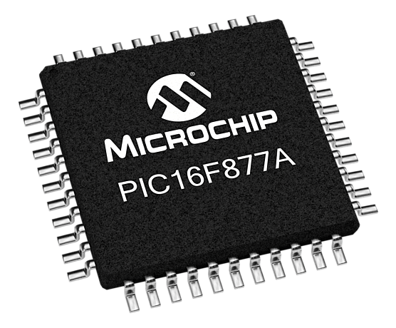
PIC16F877A Introduction
Microcontroller PIC16F877A is one of the PICmicro Family microcontrollers which is popular at this moment, start from beginner until all professionals. Because very easy to use PIC16F877A and use FLASH memory technology so that can be write-erase until thousand times. The superiority this Risc Microcontroller compared to with another microcontroller 8-bit especially at a speed of and his code compression.
The 16F877A is a capable microcontroller that can do many tasks because it has a large enough programming memory (large in terms of sensor and control projects) of 8k words and 368 Bytes of RAM. This is enough to do many different projects.
Note: There is a more modern part (the 16F887) that has nearly the same functionality as the 16F877A but also includes an internal clock – like the 16F88 and the 18F4550. In addition, the 16F887 also has low power operation using nano wattTM technology.

The four features that might make you use a 16F887 instead of a 16F877(A) are
- External gate.
- Volt Reference.
- Nano WattTM.
- Internal Clock.
The gate could be used to more accurately capture an input time e.g. for a reciprocal frequency counter.
The volt reference means you don’t need an external reference although it will probably not be useful for highly accurate operation. It is definitely more useful in a battery-powered operation where you want to compare the input battery voltage to a known reference e.g. using the comparator and the internal 0.6V reference.
Nano WattTM could be useful for battery-powered operations.
The internal clock is useful for lab development (not for accuracy) and for general operation – it can also be set to 31kHz so consuming less power.
All the above depend on your specific application requirements.
PIC16F877A has 40 pins by 33 paths of I/O. The 40 pins make it easier to use the peripherals as the functions are spread out over the pins. This makes it easier to decide what external devices to attach without worrying too much if there are enough pins to do the job.
One of the main advantages is that each pin is only shared between two or three functions so it’s easier to decide what the pin function (other devices have up to 5 functions for a pin).
A slight disadvantage of the device is that it has no internal oscillator so you will need an external crystal or another clock source. However the internal oscillator is only 1% accurate and adding a crystal (max 20MHz crystal – for 5MHz internal instruction cycle) and two 15pF capacitors is not a great chore – the accuracy will be 100ppm depending on the crystal used.
Pinout
The pinout of the 16F877A is:

Features of PIC16F877A (PIC16F877A Introduction)
The PIC16F877A CMOS FLASH-based 8-bit microcontroller is upward compatible with the PIC16C5x, PIC12Cxxx, and PIC16C7x devices. It features 200 ns instruction execution, 256 bytes of EEPROM data memory, self-programming, an ICD, 2 Comparators, 8 channels of 10-bit Analog-to-Digital (A/D) converter, 2 capture/compare/PWM functions, an asynchronous serial port that can be configured as either 3-wire SPI or 2-wire I2C bus, a USART, and a Parallel Slave Port.
High-Performance RISC CPU
- Lead-free; RoHS-compliant
- Operating speed: 20 MHz, 200 ns instruction cycle
- Operating voltage: 4.0-5.5V
- Industrial temperature range (-40° to +85°C)
- 15 Interrupt Sources
- 35 single-word instructions
- All single-cycle instructions except for program branches (two-cycle)
Special Microcontroller Features
- Flash Memory: 14.3 Kbytes (8192 words)
- Data SRAM: 368 bytes
- Data EEPROM: 256 bytes
- Self-reprogrammable under software control
- In-Circuit Serial Programming via two pins (5V)
- Watchdog Timer with on-chip RC oscillator
- Programmable code protection
- Power-saving Sleep mode
- Selectable oscillator options
- In-Circuit Debug via two pins
Peripheral Features
- 33 I/O pins; 5 I/O ports
- Timer0: 8-bit timer/counter with 8-bit Prescaler
- Timer1: 16-bit timer/counter with Prescaler
- Can be incremented during Sleep via external crystal/clock
- Timer2: 8-bit timer/counter with 8-bit period register, Prescaler, and postscaler
- Two Capture, Compare, PWM modules
- 16-bit Capture input; max resolution 12.5 ns
- 16-bit Compare; max resolution 200 ns
- 10-bit PWM
- Synchronous Serial Port with two modes:
- SPI Master
- I2C Master and Slave
- USART/SCI with 9-bit address detection
- Parallel Slave Port (PSP)
- 8 bits wide with external RD, WR, and CS controls
- Brown-out detection circuitry for Brown-Out Reset
Analog Features
- 10-bit, 8-channel A/D Converter
- Brown-Out Reset
- Analog Comparator module
- 2 analog comparators
- Programmable on-chip voltage reference module
- Programmable input multiplexing from device inputs and internal VREF
- Comparator outputs are externally accessible
If you want to see the Datasheet please visit here.
I think this PIC16F877A Introduction is more than enough to get start on PIC16F877A. In our next tutorial, we will see the PIC16F877A GPIO and LED interfacing.
You can also read the below tutorials.
Embedded Software | Firmware | Linux Devic Deriver | RTOS
Hi, I am a tech blogger and an Embedded Engineer. I am always eager to learn and explore tech-related concepts. And also, I wanted to share my knowledge with everyone in a more straightforward way with easy practical examples. I strongly believe that learning by doing is more powerful than just learning by reading. I love to do experiments. If you want to help or support me on my journey, consider sharing my articles, or Buy me a Coffee! Thank you for reading my blog! Happy learning!
