This article is a series on the Verilog – HDL and carries the discussion on Verilog HDL. The aim of this series is to provide easy and practical examples that anyone can understand. In our previous article, we have seen the introduction and history of the Verilog-HDL. In this article, we will discuss Modeling, Simulation, and Synthesis – Verilog-HDL Part 2.
Table of Contents
Modeling, Simulation, and Synthesis – Verilog-HDL Part 2
VLSI Design Flow

- The system specification is the initial step in the design flow. Is a representation of the system and specifications are the factors to be considered before constructing any design with the thought of market prerequisites and financial reasonability. The factors include size, functionality, speed, power, and performance. The next step is the architectural specification after specifying the parameters required for the VLSI system.
- Architectural specification fills in the structural details of the VLSI plan. It may be either RISC [Reduced Instruction Set Computer] or CISC [Complex Instruction Set Computer], number of ALUs, number, and structure of pipelines, Floating Point units, and size of caches.
- The behavioral or Functional Design step deals with the main functional units of the system. It represents the interconnections between the units. The behavioral aspects are determined based on the factors like input, output, and timing taken for the conduction per unit. As the result, we understand the relation between the units and this leads to overall design improvement. The use of functional design enables fast simulation and debugging of the integrated structure.
- Logic Design can also be called a Register Transfer Level (RTL) description. It can be expressed in Hardware Description Languages such as Verilog, and VHDL. The logic design comprises the Boolean expressions and arithmetic operations which can be used in the process of simulation and verification.
- Circuit design is the process of creating a circuit representation based on a logical design. The speed and power limitations of the original design are taken into account when converting the Boolean formulas into a circuit representation.
- In Physical design circuit diagram is turned into a geometrical design known as layout in this step. Each logic component (diodes, gates, transistors) is converted into a geometric representation that performs the respective intended function. Because this is a complicated process, it is run as an automated function(partially or fully) using Layout synthesis tools which can build a layout straight from a netlist.
- After getting the layout design a series of tests are now run to ensure that the designed layout functions as planned.
- Physical verification
- Logical Equivalence Checking (LEC)
- Timing Analysis
The major checks in physical verification are:
- DRC: DRC(Design Rule Check) checks assess whether the layout complies with a set of manufacturing requirements. The most prevalent are metal spacing rules, minimum width rules, via rules, and so on.
- LVS: Layout vs Schematic is another important check in the physical verification step is LVS. You’re checking that the layout you’ve developed is functionally identical to the design’s schematic/netlist. As a result, all of the connections should be in place and no connections should be missing.
- ERC: ERC (Electrical rule check) entails inspecting a design for any potentially unsafe electrical connections like floating gate errors, and VDS/VSS errors.
- The design is ready for production after layout and verification. The occurrence of data release is known as Tape Out because layout data is normally delivered to fabrication on a tape. Small wafers are made from silicon crystals. Photo-lithographic masks are created from layout data. Masks mark the locations where the elements are to be put. Because VLSI devices have such small dimensions, the wafers must be precisely polished.
- Following fabrication, packing should be done with care so that the chips meet all design parameters without being damaged. Because MCMs use bare or naked chips, chips used in Multi-Chip Modules (MCM) are not packed. Dual In-line Package (DIP), Ball Grid Array (BGA), and Quad Flat Package chips are used in printed circuit boards (PCBs) (QFP).
Hierarchical Modeling Concepts
We must first comprehend the hierarchical modeling concepts of digital design before understanding the Verilog language.
Design Methodologies
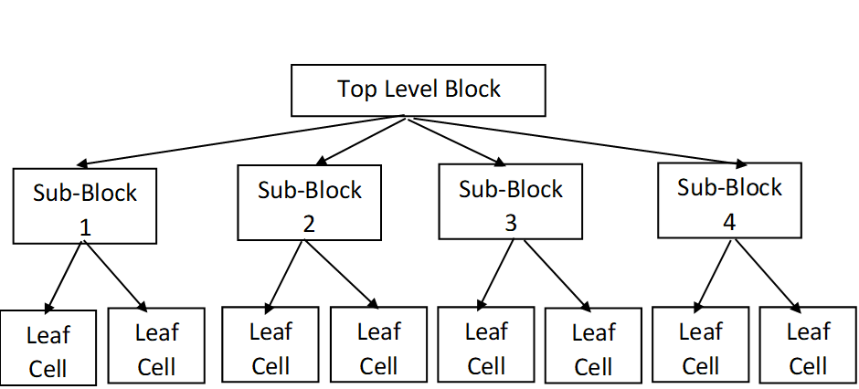
Top-Down Methodology
|
|
|
We define the top-level block and determine the sub-blocks required to construct it. We divide the sub-blocks further until we reach the leaf cells, which cannot be divided any further.
Bottom-Up Methodology
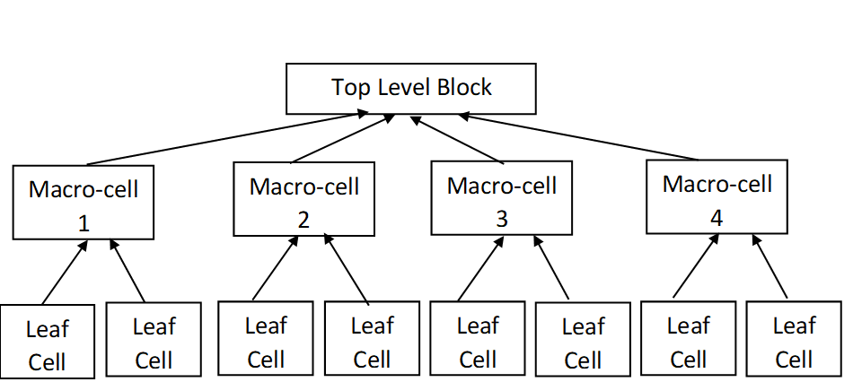
We begin by determining whatever building blocks are available to us. We use these building components to create larger cells. These cells are then used for higher-level blocks until we construct the design’s top-level block.
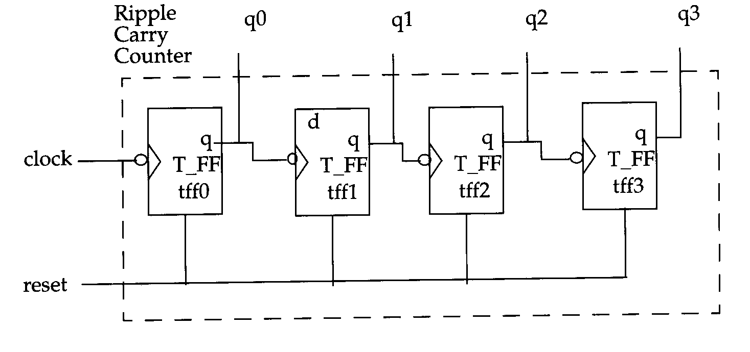
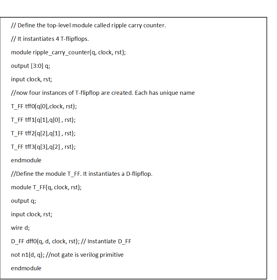
For example, see the below 4-bit Ripple Carry Counter.
|
|
|
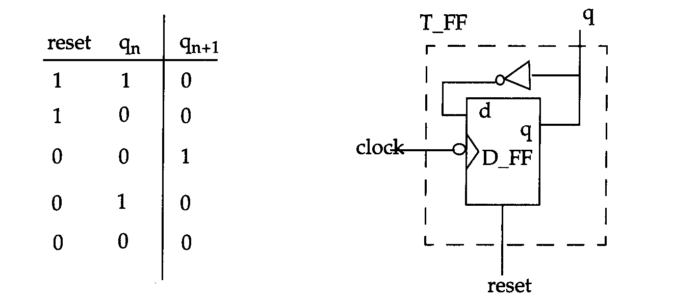
The above figure shows the ripple carry counter made up of negative edge triggered T-flipflops. Each of the T_FFs can be made up of negative edge-triggered D-flipflops and inverters.
The ripple carry counter is built in a hierarchical fashion by using building blocks.
Modules
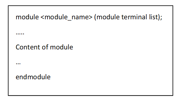
In Verilog, a module is the fundamental building block. A module can be an individual element or a grouping of lower-level design elements. Typically, items are organized into modules to give common functionality that may be used across the design.
In the above example modules include ripple-carry counter, T FF, and D FF. The keyword module is used to declare a module in Verilog. At the end of the module, the keyword endmodule must present. Each module must have a module name, which serves as the module’s identity, as well as a module terminal list, which describes the module’s input and output terminals.
|
|
|
Each module’s internals can be described at four degrees of abstraction, depending on the design’s requirements.
- The highest level of abstraction in Verilog HDL is the behavioral or algorithmic level.
- Dataflow level is the data flow is specified when the module is created.
- Logic gates and linkages are used to implement the module at the gate level.
- Switch level is the lowest level of abstraction, implemented in terms of switches, storage nodes, and their interconnections.
In a Verilog design, the designer can mix and match all four levels of abstraction. A mix of behavioral and dataflow constructs is used to define the term register transfer level (RTL). The higher the level of abstraction, the more flexible and technology-agnostic the design is but as one descends into the switch-level design, the design becomes increasingly technology-dependent and inflexible.
Instances
A module serves as a starting point for creating actual things. Verilog builds a unique object from the template when a module is called. The name, variables, parameters, and I/O interface of each object are unique. Instantiation is the process of constructing objects from a module template, and the objects are known as instances.
For example:
|
|
|
It is illegal to nest modules in Verilog. Within the module and endmodule commands, one module declaration cannot contain another module definition. Instead, a module definition can instantiate other modules to include copies of them. Module descriptions simply describe how a module will function, including its internals and interface. For use in the design, modules must be instantiated. Nesting modules are forbidden in Verilog. Within the module and endmodule commands, one module declaration cannot contain another module definition. Instead, a module definition can instantiate other modules to include copies of them. Module descriptions simply describe how a module will function, including its internals and interface. For use in the design, modules must be instantiated.
Components of Simulation
A design block must be tested once it has been completed. The design block’s functionality can be tested by applying stimuli and observing the results. This type of block is known as a stimulus block, and it can be written in Verilog as a test bench. To completely test the design block, many test benches might be employed.

In the figure above stimulus, the block becomes the top-level block. It manipulates signals clock and reset(rst), and it checks and displays output signal q.
|
|
|
The second method of applying stimulus is to use a top-level dummy module to instantiate both the stimulus and design blocks. The interface is the only way for the stimulus block to communicate with the design block.
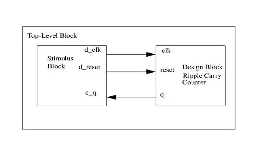
The d_clk and d_reset signals are driven by the stimulus module. Signal c_q is also checked and shown. The design and stimulus blocks are simply instantiated by the top-level block. Either type of stimulus can be effective.
In our next tutorial, we will discuss lexical tokens in Verilog.
You can also read the below tutorials.
|
|
|

Electronics and Communication Engineer
