When I was a newbie in Embedded Systems, I used to wonder how the microcontroller is communicating with other devices like sensors, displays, and SD cards, etc. I heard about UART already, but not the SPI, and I2C. Then I got to know that, there are many other serial communications are available other than UART. Many people will be out there like me. We have posted the I2C Basics already. So, in this post, we will focus on SPI – Serial Peripheral Interface Protocol Basics, SPI Bus protocol Modes, Daisy chain in SPI, etc.
Table of Contents
What is the SPI serial interface?
We had discussed earlier about serial communication. SPI is one of the most popular serial communication protocols. SPI – Serial Peripheral Interface is an interface bus commonly used to transmit and receive the data between microcontrollers and small peripherals such as shift registers, sensors, displays, flash memory, etc. Since it is synchronous communication, it uses a separate clock line and data lines. The interface was developed by Motorola in the mid-1980s.
SPI Specification
An SPI – Serial Peripheral Interface protocol system consists of one master device and one or more slave devices. But in I2C, we can have one or more master devices and one or more slave devices. The master is providing the SPI clock and the slave is receiving the SPI clock from the master.
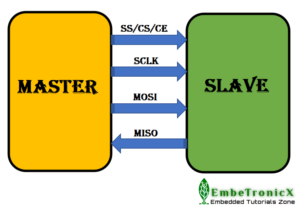
SPI needs 4 wires at least. But some of the recent day devices support 3 pin mode and 4pin modes also.
- MOSI – Master Out Slave In
- MISO – Master In Slave Out
- SCLK – Serial Clock
- SS/CS/CE – Salve Select/Chip Select/Chip Enable
|
|
|
- MOSI – Master Out Slave In is used to send the data from the master to the slave device.
- MISO – Master In Slave Out is used to receive the data from the slave to the master device.
- SCLK – Serial Clock is the clock that is generated by the master device.
- SS/CS/CE – Salve Select/Chip Select/Chip Enable line is used to select the slave device in the SPI bus interface.
SPI protocol is a Full-duplex as this protocol has separate pins for incoming data and outgoing data. So, we can transmit and receive the data at the same time.
Note: on a slave-only device, MOSI may be labeled as SDI (Serial Data In) and MISO may be labeled as SDO (Serial Data Out).
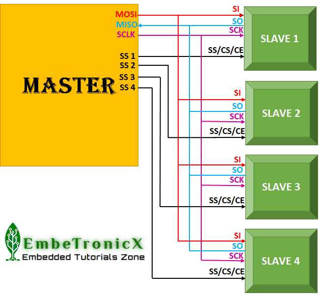
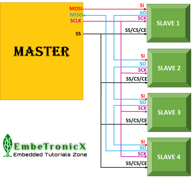
When you increase the number of slaves, then the Slave Select pin also increases. You can easily understand this logic by using the below image.
If you see the above picture, the master device has to use the 7 pins for 4 slave devices. Yes, I can hear you. This is one of the disadvantages. In I2C, the number of pins won’t increase even if you increase the slave devices. To avoid this scenario, they have introduced daisy chain logic. We will discuss that daisy chain later in this post.
|
|
|
The communication (data transmission between the master and the slave) is synchronized to the clock generated by the master. So, as it is synchronized using the clock, it doesn’t have to wait for a response before doing other operations. SPI devices support much higher clock frequencies compared to I2C interfaces.
Data Transmission
To begin communication, the bus master configures the clock, using a frequency supported by the slave device, typically up to a few MHz. Once the clock has been configured, then the master makes the Slave select (SS/CS) pin LOW that initiates the transfer. When multiple slaves are used, the master has to make the respective slave’s Slave select (SS/CS) pin LOW.
During each SPI clock cycle, full-duplex data transmission occurs. The master sends a bit on the MOSI pin and the slave reads it, while the slave sends a bit on the MISO pin and the master reads it. This sequence is maintained even when only one-directional data transfer is intended.
Transmissions normally involve two shift registers of eight bits (mostly but size varies based on the slaves), one in the master and one in the slave. Data is usually shifted out with the most significant bit (MSB) first. On the clock edge, both master and slave shift out a bit and output it on the transmission line to the counterpart. On the next clock edge, at each receiver, the bit is sampled from the transmission line and set as a new least-significant bit of the shift register. After the register bits have been shifted out and in, the master and slave have exchanged register values. If more data needs to be exchanged, the shift registers are reloaded and the process repeats. Transmission may continue for any number of clock cycles.
Refer to the below image for your understanding.
|
|
|
When the master completes the data transfer, then the master stops toggling the clock signal and it makes the SS/CS pin HIGH.
SPI Modes
The SPI interface defines no protocol for data exchange, limiting overhead and allowing for high-speed data streaming. We saw how the data is being transferred to the slave from the master. As we have an understanding of data communication, let’s go a little bit deeper. In addition to setting the clock frequency, the master must also configure the clock polarity and phase with respect to the data. Clock polarity (CPOL) and clock phase (CPHA) are the two parameters that are used to form four unique modes to provide flexibility in communication between master and slave.
| CPOL | CPHA | MODE |
| 0 | 0 | MODE 0 |
| 0 | 1 | MODE 1 |
| 1 | 0 | MODE 2 |
| 1 | 1 | MODE 3 |
Everything is going well in SPI. But, why did they create these modes? If you see in I2C, whenever the clock (SCL) is going low, that time data will be changed, and when the clock (SCL) is high, that time data will be sampled. Right? Not understood? Okay, refer to the below image. You will understand.
|
|
|
In the above image, the yellow color is START and STOP condition. Blue colors are where the data is being changed when SCL is Low. And the Green colors are where the data is read by the slave or master when SCL is High. So, these data changing and sampling place is fixed in the I2C. But in SPI, it is not fixed. It is flexible and the CPOL and CPHA are used to tell the master and slave that when to sample the data. I guess you must be clear now.
The clock polarity (CPOL) determines the initial state of the Clock pin (SCLK). If CPOL is 0 means then the SCLK line’s initial state is Low, and if CPOL is 1 means the SCLK line’s initial state is High.
The clock phase (CPHA) determines the edge. If CPHA is 0 then it means the leading edge (1st edge), and if CPHA is 1, then it means the trailing edge (2nd edge). These edges can be high to low or low to high.
Let’s see the modes.
Mode 0
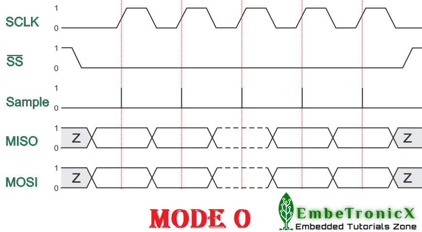
In this mode, CPOL is 0 and CPHA is also 0. So, the SCLK starts as Low and the data will be sampled at the first edge. Check the below image to understand that.
|
|
|
The data must be available before the first clock signal rising. The clock idle state is LOW. The data on MISO and MOSI lines must be stable while the clock is high and can be changed when the clock is low. The data is captured on the clock’s low-to-high transition and can be propagated on high-to-low clock transition.
Mode 1
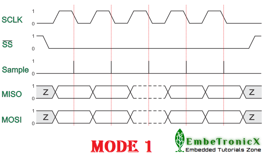
In this mode, CPOL is 0 and CPHA is also 1. So, the SCLK starts as Low and the data will be sampled at the second edge. Check the below image.
The first clock signal rising can be used to prepare the data. The clock idle state is LOW. The data on MISO and MOSI lines must be stable while the clock is low and can be changed when the clock is high. The data is captured on the clock’s high-to-low transition and propagated on low-to-high clock transition.
|
|
|
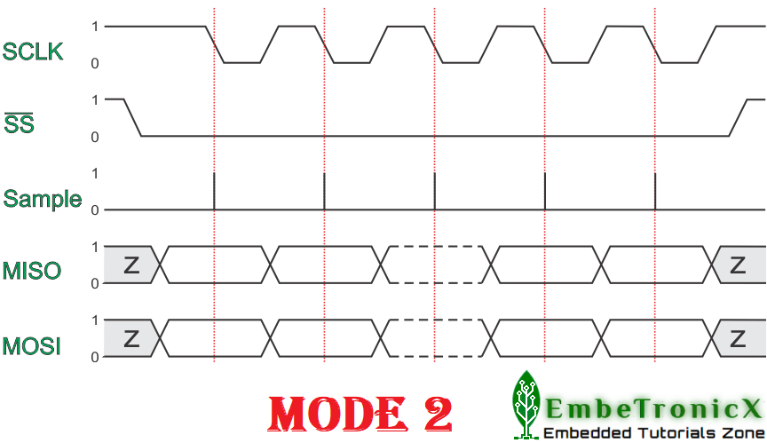
Mode 2
In this mode, CPOL is 1 and CPHA is also 0. So, the SCLK starts as High and the data will be sampled at the first edge. Check the below image to understand that.
The data must be available before the first clock signal falling. The clock idle state is HIGH. The data on MISO and MOSI lines must be stable while the clock is low and can be changed when the clock is high. The data is captured on the clock’s high-to-low transition and propagated on low-to-high clock transition.
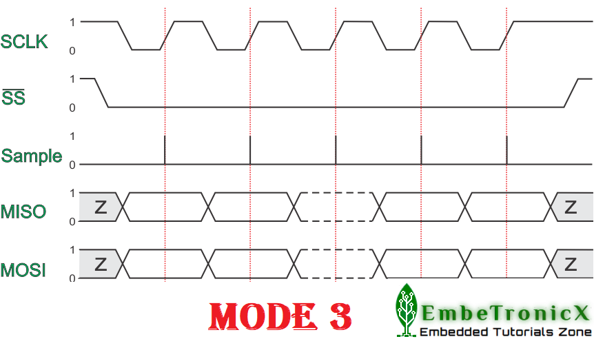
Mode 3
In this mode, CPOL is 1 and CPHA is also 1. So, the SCLK starts as High and the data will be sampled at the second edge. Check the below image to understand that.
|
|
|
The first clock signal falling can be used to prepare the data. The clock idle state is HIGH. The data on MISO and MOSI lines must be stable while the clock is high and can be changed when the clock is low. The data is captured on the clock’s low-to-high transition and propagated on high-to-low clock transition.
I hope, now you must have a fair idea about the SPI modes.
Now, some people might think that, Is there any way to reduce the Pins that are used for the SPI communications? Yes, there are certain scenarios we can apply to reduce the pins.
- When you have only one slave, then you can directly connect the SS/CS pin to the ground if your slave permits it. This trick may not work for some slaves as those slaves require a falling edge of the chip select signal to initiate an action. Ex: Maxim MAX1242 ADC.
- When you have only one slave, that only gets the data from the master and it won’t send anything to the master, then you can leave the MISO pin.
- When you have multiple slaves, then you can use an external decoder/demultiplexer. Ex: 74HC4515.
- When you don’t want to use an external decoder/demultiplexer, then you can think of the daisy chain approach.
Daisy Chain
In the Daisy chain method, we can use a single SS/CS line for all the slaves like below.
|
|
|
If you closely look at the above image, We made two modifications to the normal SPI connections.
- Removed the other SS/CS pins and connected all the slave’s SS/CS pin to the one SS/CS pin of the master.
- All the slave’s Output (SO) is connected to the next slave’s input (SI) and the last slave’s output is connected to the master’s MISO.
That’s all. Our daisy chain circuit is ready.
How Daisy Chaining Is Accomplished?
The daisy chain circuit is cool bro. But How it is actually working? Okay, I have the answer for you.
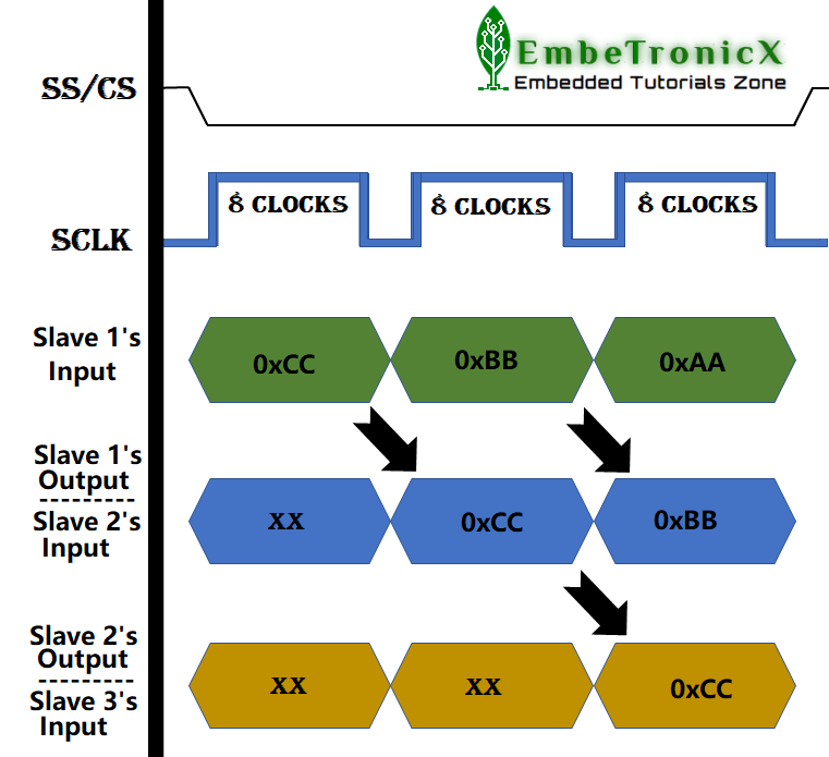
Slave 1’s input (SI) is directly connected to the master’s MOSI. When the master transmits the data, it will be stored in slave 1’s internal shift register for the first 8 clock cycles. Then in the next 8 clock cycles, slave 1 will be sent out the data from its internal shift register through its output (SO). As Slave 1’s output (SO) line is connected to Slave 2’s input (SI), Slave 2 will receive the data in the next 8 clock cycles. And this process continues as long as the master generating the clocks and SS/CS line is Low.
I know, a picture speaks a lot than the theory. Check the below example with the picture.
|
|
|
Assume that the master wants to send 0xAA to slave 1, 0xBB to slave 2, and 0xCC to slave 3. The below picture explains what happens in each 8 clock cycle.
In this method, as data is propagated from one slave to the next, the number of clock cycles required to transmit data is proportional to the slave position in the daisy chain. In the above example, if the master wants to send the 8-bits of data to Slave 3, then it takes 24 clock cycles. If you have used the normal SPI mode instead of the daisy chain, then the master would just take 8 clock cycles to send 8-bit data instead of the 24 clock cycles.
Daisy-chain mode is not necessarily supported by all SPI devices. Please refer to the product datasheet to confirm if the daisy chain is available.
Advantages of SPI
- It’s way faster than asynchronous serial communication and I2C (almost twice as fast).
- No start and stop bits, so the data can be streamed continuously without interruption.
- No slave addressing mechanism like I2C.
- It has separate MISO and MOSI lines, so data can be sent and received at the same time (Full duplex).
- Not Limited to 8-bit data.
- The received hardware (slave) can be a simple shift register.
- It supports multiple slave devices.
Disadvantages of SPI
- It requires more lines (wires) than other communication methods. (UART and I2C only require 2 lines).
- There is no acknowledgment to inform that data has been successfully transferred like I2C and No error detection protocol is defined.
- The communications must be well-defined in advance (you can’t send random amounts of data whenever you want).
- The master must control all communications (slaves can’t talk directly to each other).
- It usually requires separate CS lines to each peripheral, which can be problematic if numerous slaves are needed.
- SPI only supports a single master.
- Can be used only from short distances.
Applications
- SPI is used to talk to a variety of peripherals, such as,
- Sensors: temperature, pressure, ADC, touchscreens, video game controllers
- Control devices: audio codecs, digital potentiometers, DAC
- Camera lenses: Canon EF lens mount
- Communications: Ethernet, USB, USART, CAN, IEEE 802.15.4, IEEE 802.11, handheld video games
- Memory: flash and EEPROM
- Real-time clocks
- LCD
- Any MMC or SD card
I2C vs SPI
It is really worth comparing the two synchronous serial communications I2C and SPI. We have posted a separate post for I2C. You can read the I2C Basics and advanced concepts.
|
|
|
| I2C | SPI |
| I2C has been developed in 1982 by Philips Semiconductors (NXP). | SPI is developed by Motorola in the mid-1980s. |
| It supports multi masters. | It supports only one master. |
| It needs a maximum of 2 wires. | It needs a minimum of 4 wires and the maximum is based on the number of slaves. |
| It is half-duplex communication as it has only one wire for Tx and Rx. | It is full-duplex communication as it has separate wires for Rx and Tx. |
| It is slower than the SPI. | It is faster than the I2C. |
| I2C has an acknowledgment mechanism. | This doesn’t have an acknowledgment mechanism. |
| In this protocol, the slave has to have a unique address. | In this protocol, the slave doesn’t need an address. Master will use the SS/CS wire to select the slaves. |
| Due to Start, Stop, Address bits, it has overhead. | But it will directly start the data transfer. Start and Stop are not required. So, no overhead here. |
| I2C is better for long-distance. | SPI is better for a short distance. |
You can also read the below tutorials.

Embedded Software | Firmware | Linux Devic Deriver | RTOS
Hi, I am a tech blogger and an Embedded Engineer. I am always eager to learn and explore tech-related concepts. And also, I wanted to share my knowledge with everyone in a more straightforward way with easy practical examples. I strongly believe that learning by doing is more powerful than just learning by reading. I love to do experiments. If you want to help or support me on my journey, consider sharing my articles, or Buy me a Coffee! Thank you for reading my blog! Happy learning!

