This article is the first part of the Series on the ESP32 Tutorials using ESP-IDF and carries the discussion on the ESP32 and its peripherals. The aim of this series is to provide easy and practical examples that anyone can understand. In this post, we will see ESP32 Introduction and Initial Process Flow.
Table of Contents
ESP32 Introduction and Initial Process Flow
Introduction
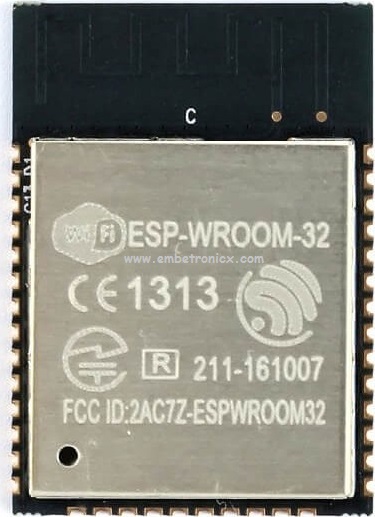
The ESP-WROOM-32 Wifi Bluetooth combo module is ultra-high performance and ultra-low power consumption FCC-approved (2AC7Z-ESPWROOM32) Wi-Fi and Bluetooth combo wireless platform based on ESPRESSIF ESP32 chipset. It integrates a dual-core processor, 448 KByte ROM,520 KByte SRAM,16 KByte SRAM in RTC, 802.11 b/g/n/e/I Wi-Fi, Bluetooth v4.2 BR/EDR & BLE, clocks & Times, abundant peripheral Interfaces, and security mechanism.
Architecture
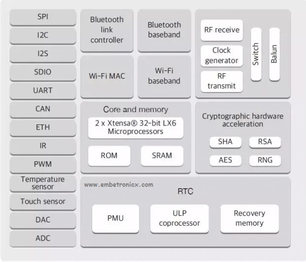
The ESP-WROOM-32 Wifi Bluetooth combo module provides SDK Firmware for fast online programming and open-source toolchains based on GCC for development support. It is designed for Generic low power IoT sensor hubs, loggers, video steaming for cameras, Wi-Fi & Bluetooth enabled devices, Home automation, and mesh network applications, aimed at makers, hardware engineers, software engineers, and solution providers. ESP32 is a single-chip 2.4 GHz Wi-Fi and Bluetooth combo chip designed with TSMC ultra-low-power 40 nm technology. It is designed and optimized for the best power performance, RF performance, robustness, versatility, features, and reliability, for a wide variety of applications, and different power profiles.
ESP32 is the most integrated solution for Wi-Fi + Bluetooth applications in the industry with less than 10 external components. ESP32 integrates the antenna switch, RF balun, power amplifier, low noise receive amplifier, filters, and power management modules. As such, the entire solution occupies a minimal Printed Circuit Board (PCB) area. ESP32 is designed for mobile, wearable electronics, and Internet of Things (IoT) applications. It has many features of state-of-the-art low-power chips, including fine-resolution clock gating, power modes, and dynamic power scaling.
|
|
|
Key Features
- CPU and Memory: Xtensa® 32-bit LX6 Dual-core processor, up to 600 DMIPS.
- 448 KByte ROM
- 520 KByte SRAM
- 16 KByte SRAM in RTC.
- SPI can connect up to 4* Flash/SRAM, each flash should be less than 16 Mbytes.
- Supply Voltage: 2.2V~3.6V
WiFi
- 802.11 b/g/n/e/i
- WMM-PS, UAPSD
- 802.11 e: QoS for wireless multimedia technology.
- 802.11 n (2.4 GHz), up to 150 Mbps
- MPDU and A-MSDU aggregation
- Block ACK
- Fragmentation and defragmentation
- Automatic Beacon monitoring/scanning
- 802.11 i security features: pre-authentication and TSN
- Wi-Fi Protected Access (WPA)/WPA2/WPA2-Enterprise/Wi-Fi Protected Setup (WPS)
- Infrastructure BSS Station mode/SoftAP mode
- Wi-Fi Direct (P2P), P2P Discovery, P2P Group Owner mode, and P2P Power Management
- UMA compliant and certified
- Antenna diversity and selection
Bluetooth
- Compliant with Bluetooth v4.2 BR/EDR and BLE specification
- Class-1, class-2, and class-3 transmitter without external power amplifier
- Enhanced power control
- +10 dBm transmitting power
- NZIF receiver with -98 dBm sensitivity
- Adaptive Frequency Hopping (AFH)
- Standard HCI based on SDIO/SPI/UART? High-speed UART HCI, up to 4 Mbps
- BT 4.2 controller and host stack
- Service Discover Protocol (SDP)
- General Access Profile (GAP)
- Security Manage Protocol (SMP)
- Bluetooth Low Energy (BLE)
- ATT/GATT
- HID
- All GATT-based profiles supported
- SPP-Like GATT-based profile
- BLE Beacon
- A2DP/AVRCP/SPP, HSP/HFP, RFCOMM
- CVSD and SBC for audio codec
- Bluetooth Piconet and Scatternet
Clocks and Timers
- Internal 8 MHz oscillators with calibration
- Internal RC oscillator with calibration
- External 2 MHz to 40 MHz crystal oscillator
- External 32 kHz crystal oscillator for RTC with calibration
- Two timer groups, including 2 x 64-bit timers and 1 x main watchdog in each group
- RTC watchdog
Peripheral Interface
- 12-bit SAR ADC up to 18 channels
- 2 × 8-bit D/A converters
- 10 × touch sensors
- Temperature sensor
- 4 × SPI, 2 × I2S, 2 × I2C, 3 × UART
- 1 host (SD/eMMC/SDIO), 1 slave (SDIO/SPI)
- Ethernet MAC interface with dedicated DMA and IEEE 1588 support
- CAN 2.0
- IR (TX/RX)
- Motor PWM, LED PWM up to 16 channels
- Hall sensor
- Ultra-low power analog pre-amplifier
Security
- IEEE 802.11 standard security features all supported, including WFA, WPA/WPA2, and WAPI
- Secure boot
- Flash encryption
- 1024-bit OTP, up to 768-bit for customers
- Cryptographic hardware acceleration: -AES-HASH(SHA-2) library-RSA-ECC-Random Number Generator (RNG)
Development Support
- SDK Firmware for fast online programming
- Open source toolchains based on GCC
Applications
- Generic low power IoT sensor hub
- Generic low power IoT loggers
- Video streaming from camera
- Over The Top (OTT) devices
- Music players – Internet music players – Audio streaming devices
- Wi-Fi enabled toys – Loggers – Proximity sensing toys
- Wi-Fi enabled speech recognition devices
- Audio headsets
- Smart power plugs
- Home automation
- Mesh network
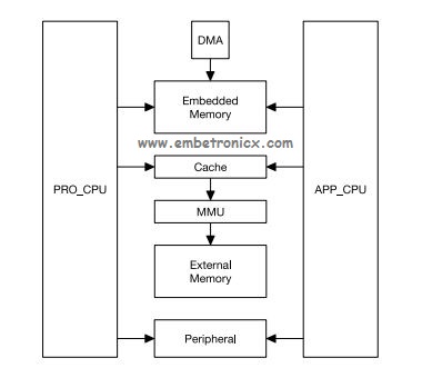
Also, one interesting thing to note is that both processors are mapped symmetrically to this address space. It basically means, a register for example can be accessed from the same address location from both the CPUs as shown in the image below.
This note explains various steps which happen before the app_main function of an ESP-IDF application is called.
Process Flow
- ROM Bootloader (First Bootloader) loads the second bootloader to RAM.
- The second bootloader loads the partition table and main_app image from flash.
- Main app image excutes.At this point, the second CPU and RTOS scheduler can be started.
1. ROM Bootloader (First Bootloader)
After SoC reset, PRO CPU will start running immediately, executing the reset vector code, while APP CPU will be held in reset. During the startup process, PRO CPU does all the initialization. APP CPU reset is de-asserted in the call_start_cpu0 function of the application startup code.
Startup code called from the reset vector determines the boot mode by checking GPIO_STRAP_REGregister for bootstrap pin states. Depending on the reset reason, the following takes place:
|
|
|
1. For power-on reset, software SOC reset, and watchdog SOC reset
check the GPIO_STRAP_REGregister if UART or SDIO download mode is requested. If this is the case, configure UART or SDIO, and wait for the code to be downloaded. Otherwise, proceed with the boot.
2. For software CPU reset and watchdog CPU reset
attempt to load the code from flash. If loading code from flash fails, unpack BASIC interpreter into the RAM and start it. Note that the RTC watchdog is still enabled when this happens, so unless any input is received by the interpreter, the watchdog will reset the SOC in a few hundred milliseconds, repeating the whole process. If the interpreter receives any input from the UART, it disables the watchdog.
Application binary image is loaded from flash starting at address 0x1000. The First 4kB sector of flash is used to store secure boot IV and the signature of the application image.
2. Second Bootloader
In ESP-IDF, the binary image which resides at offset 0x1000 in flash is the second stage bootloader. When the first stage bootloader is finished checking and loading the second stage bootloader, it jumps to the second stage bootloader entry point found in the binary image header. The second stage bootloader reads the partition table found at offset 0x8000. The bootloader finds factory and OTA partitions and decides which one to boot based on data found in the OTA info partition. The second stage bootloader configures flash MMU for both PRO and APP CPUs, but it only enables flash MMU for PRO CPU.
Once code is loaded and flash MMU is set up, the second stage bootloader jumps to the application entry point found in the binary image header.
|
|
|
3. Application startup
ESP-IDF application entry point is call_start_cpu0 function found in components/esp32/cpu_start.c. Two main things this function does are to enable heap allocator and to make APP CPU jump to its entry point, call_start_cpu1. The code on PRO CPU sets the entry point for APP CPU, de-asserts APP CPU reset, and waits for a global flag to be set by the code running on APP CPU, indicating that it has started. Once this is done, PRO CPU jumps to start_cpu0 function, and APP CPU jumps to start_cpu1 function.
While PRO CPU does initialization in start_cpu0 function, APP CPU spins in start_cpu1 function, waiting for the scheduler to be started on the PRO CPU. Once the scheduler is started on the PRO CPU, code on the APP CPU starts the scheduler as well.
The main task is the task that runs app_main function. The main task stack size and priority can be configured in menuconfig. The application can use this task for initial application-specific setup, for example, to launch other tasks. The application can also use the main task for event loops and other general-purpose activities. If the app_main function returns, the main task is deleted.
In our next article, we will see how to set up the ESP-IDF environment.
|
|
|
You can also read the below tutorials.
Embedded Software | Firmware | Linux Devic Deriver | RTOS
Hi, I am a tech blogger and an Embedded Engineer. I am always eager to learn and explore tech-related concepts. And also, I wanted to share my knowledge with everyone in a more straightforward way with easy practical examples. I strongly believe that learning by doing is more powerful than just learning by reading. I love to do experiments. If you want to help or support me on my journey, consider sharing my articles, or Buy me a Coffee! Thank you for reading my blog! Happy learning!
