
This article is a continuation of the series of tutorials on the LPC2148 Microcontroller (ARM7). The aim of this series is to provide easy and practical examples that anyone can understand. In the previous tutorial, we have seen LPC2148 (ARM7) UART. Now, we will see LPC2148 ADC Tutorial…
Table of Contents
Suggestion to read
LPC2148 ADC Tutorial
Introduction
Microcontrollers are very useful especially when it comes to communicating with other devices, such as sensors, motors, switches, memory, and even another microcontroller. As we all know many interface methods have been developed over years to solve the complex problems of balancing needs of features, cost, size, power consumption, reliability, etc. but the ADC Analog-to-Digital converter remains famous among all. Using this ADC we can connect any type of Analog sensor.
LPC2148 ADC
LPC2148 has two inbuilt 10-bit Successive Approximation ADC. ADC0 has six channels (AD0.1-AD0.6). ADC1 has 8-Channels (AD1.0-AD1.7). ADC operating frequency is 4.5 MHz (max.), operating frequency decides the conversion time.
The ADC reference voltage is measured across GND to VREF, meaning it can do the conversion within this range. Usually, the VREFPis connected to VDD.
Features
- 10-bit successive approximation analog to digital converter (one in LPC2141/2 and two in LPC2144/6/8).
- Input multiplexing among 6 or 8 pins (ADC0 and ADC1).
- Power-down mode.
- Measurement range 0 V to VREF (typically 3 V; not to exceed VDDA voltage level).
- 10 bit conversion time ≥2.44 µs.
- Burst conversion mode for single or multiple inputs.
- Optional conversion on transition on input pin or Timer Match signal.
- Global Start command for both converters (LPC2144/6/8 only).
As LPC2148 works on 3.3 volts, this will be the ADC reference voltage.
Now the Resolution of ADC = 3.3/(2^{10}) = 3.3/1024 =0.003222 = 3.2mV
|
|
|
ADC Pins In LPC2148
Let’s have a look at the table which illustrate ADC related channels and pins:
ADC0
| ADC Channel | Pin Number | Functions of that Pin | Associated PINSEL Register Bits |
|---|---|---|---|
| ADC 0.1 | P0.28 | GPIO, AD0.1, CAP0.2, MAT0.2 | 24,25 bits of PINSEL1 |
| ADC 0.2 | P0.29 | GPIO, AD0.2, CAP0.3, MAT0.3 | 26,27 bits of PINSEL1 |
| ADC 0.3 | P0.30 | GPIO, AD0.3, EINT3, CAP0.0 | 28,29 bits of PINSEL1 |
| ADC 0.4 | P0.25 | GPIO, AD0.4, AOUT | 18,19 bits of PINSEL1 |
| ADC 0.6 | P0.4 | GPIO, SCK0, CAP0.1 , AD0.6 | 08,09 bits of PINSEL0 |
| ADC 0.7 | P0.5 | GPIO, MISO0, MAT0.1 , AD0.7 | 10,11 bits of PINSEL0 |
ADC1
| ADC Channel | Pin Number | Functions of that Pin | Associated PINSEL Register Bits |
|---|---|---|---|
| ADC 1.0 | P0.6 | GPIO, MOSI0, CAP0.2, AD1.0 | 12,13 bits of PINSEL0 |
| ADC 1.1 | P0.8 | GPIO, TXD1, PWM4, AD1.1 | 16,17 bits of PINSEL0 |
| ADC 1.2 | P0.10 | GPIO, RTS1, CAP1.0, AD1.2 | 20,21 bits of PINSEL1 |
| ADC 1.3 | P0.12 | GPIO, DSR1, MAT1.0, AD1.3 | 24,25 bits of PINSEL1 |
| ADC 1.4 | P0.13 | GPIO, DTR1, MAT1.1 , AD1.4 | 26,27 bits of PINSEL3 |
| ADC 1.5 | P0.15 | GPIO, RI1, EINT2 , AD1.5 | 30,31 bits of PINSEL3 |
| ADC 1.6 | P0.21 | GPIO, PWM5, AD1.6, CAP1.3 | 10,11 bits of PINSEL1 |
| ADC 1.7 | P0.22 | GPIO, AD1.7, CAP0.0, MAT0.0 | 12,13 bits of PINSEL1 |
Registers Used For ADC
There are several registers that will be used to set up and configure the ADC feature in LPC2148. The two registers we will be concerned about: ADCR (A/D Control Register) and ADGDR (A/D Global Data register).
| Register | Description |
|---|---|
| ADxCR | A/D COntrol Register: Used for Configuring the ADC |
| ADxGDR | A/D Global Data Register: This register contains the ADC’s DONE bit and the result of the most recent A/D conversion |
| ADxINTEN | A/D Interrupt Enable Register |
| ADxDR0 - ADxDR7 | A/D Channel Data Register: Contains the recent ADC value for respective channel |
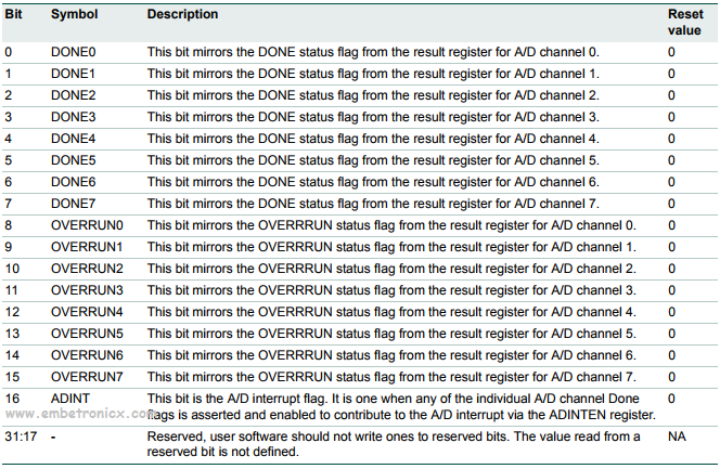
| ADxSTAT | A/D Status Register: Contains DONE & OVERRUN flag for all the ADC channels |
| ADxGSR | A/D Global Start Register: This address can be written (in the AD0 address range) to start conversions in both A/D converters simultaneously. |
|
|
|
Note : x = 0/1 (ie ADC0 or ADC1)
Here we will see only ADC0. But ADC1 also the same as ADC0 except for the Register name.
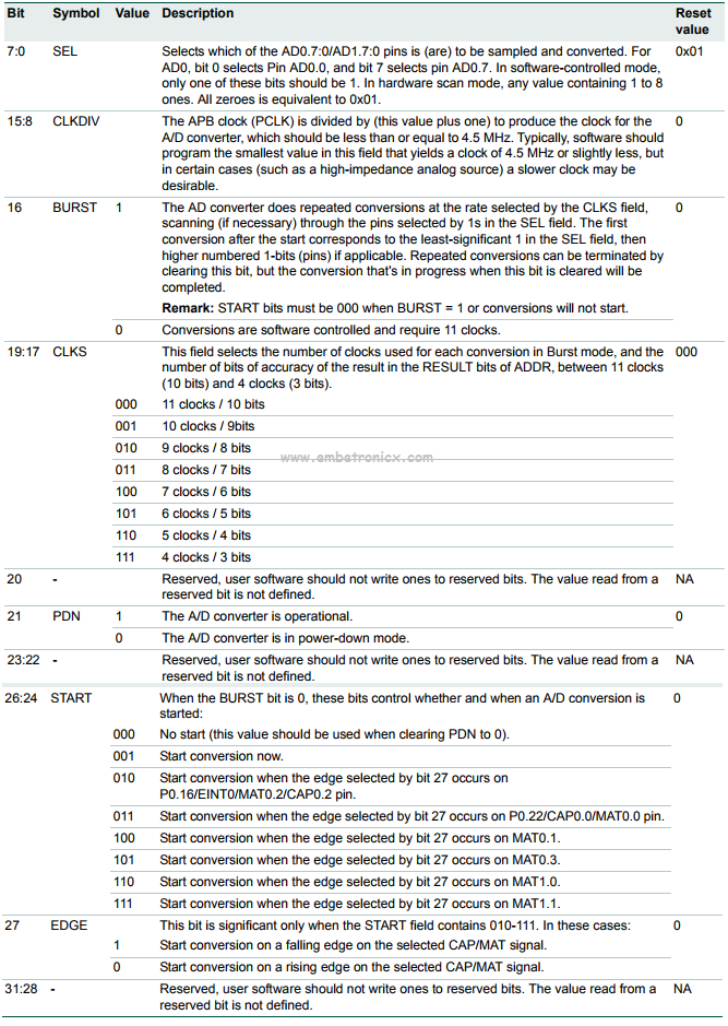
AD0CR – A/D Control Register
This is the main control register for AD0. Used for Configuring the ADC0.
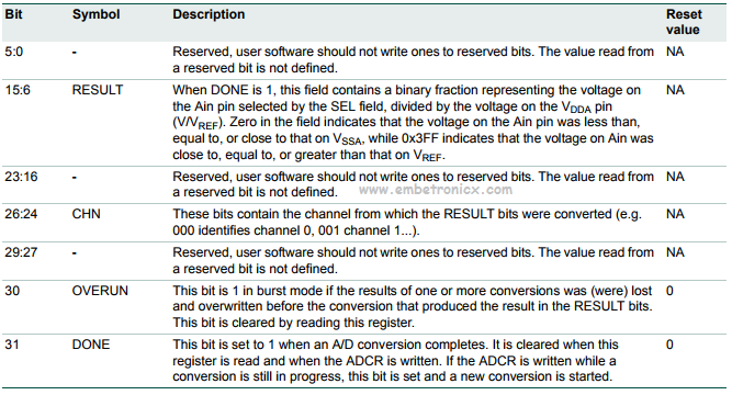
AD0GDR – A/D Global Data Register
This is the global data register for the corresponding ADC module. It contains the ADC’s DONE bit and the result of the most recent A/D conversion.
|
|
|
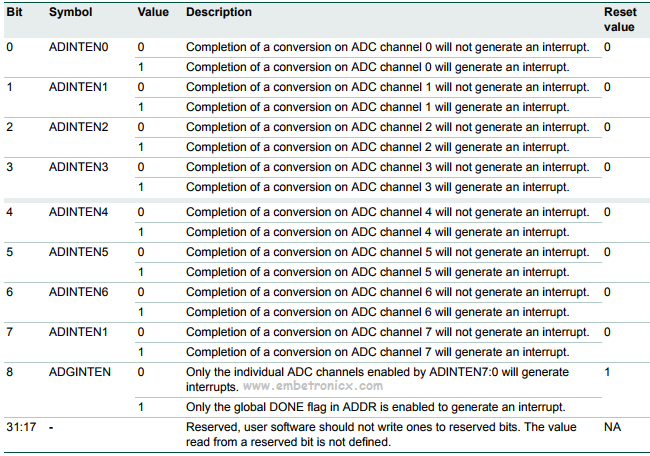
AD0INTEN – A/D Interrupt Enable Register
Using this register interrupts can be enabled or disabled for any ADC channels.
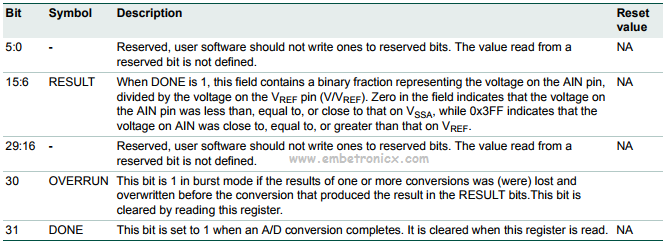
AD0DR0 to AD0DR7 – A/D Data registers
This register contains the result of the most recent conversion completed on the corresponding channel [0 to 7].
|
|
|
AD0STAT – A/D Status register
This register contains DONE and OVERRUN flags for all of the A/D channels along with the A/D interrupt flag.
AD0GSR – A/D Global Start Register
This register is used to simultaneously start the conversion process of both ADC modules.

Note: Though there are some more registers, we are restricting ourselves to use these registers only as this will be more convenient.
|
|
|
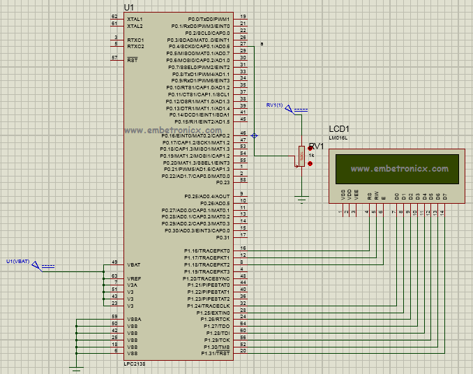
Circuit Diagram
LCD:
- RS: P1.16
- RW: P1.17
- EN: P1.18
- Data Lines: P1.24 – P1.31
ADC:
- P0.4 (ADC0.6) : Potentiometer
Programming Algorithm
Below are the steps for configuring the LPC1768 ADC.
- Configure the GPIO pin for the ADC function using the PINSEL register.
- Enable the CLock to ADC module.
- Power on the internal ADC module by setting ADCR.PDN bit (ADCR’s 21st bit).
- Select the Particular channel for A/D conversion by setting the corresponding bits in ADCR.SEL (bit 0 – bit 7).
- Set the ADCR.START bit for starting the A/D conversion for the selected channel (ADCR’s 24th bit).
- Wait for the conversion to complete, ADGDR. The DONE bit will be set once the conversion is over.
- Read the 10-bit A/D value from ADGdR.RESULT.
Code
In our tutorial, we are using ADC0.6 (ADC0 6th channel). So P0.4 is a pin for that ADC0.6.
|
|
|
You can download this project from here.
Code.c
#include<lpc214x.h>
#include "LCD.h"
#include "ADC.h"

unsigned int val;

int main()
{
    IO1DIR=0xffffffff;
    IO0DIR=0x00000000;
    PINSEL0=0x0300;
    VPBDIV=0x02;
    lcd_init();
    show("ADC Value : ");
    while(1) {
        cmd(0x8b);
        val=adc(0,6);
        dat((val/1000)+48);
        dat(((val/100)%10)+48);
        dat(((val/10)%10)+48);
        dat((val%10)+48);
    }
}
ADC.H
unsigned int val;
unsigned int adc(int,int);

unsigned int adc(int no,int ch)
{
    switch(no)                                    //select adc
    {
        case 0: AD0CR=0x00200600|(1<<ch);       //select channel
                AD0CR|=(1<<24);                 //start conversion
                while((AD0GDR& (1<<31))==0);
                val=AD0GDR;
                break;

        case 1: AD1CR=0x00200600|(1<<ch);       //select channel
                AD1CR|=(1<<24);                 //start conversion
                while((AD1GDR&(1<<31))==0);
                val=AD1GDR;
                break;
    }
    val=(val >> 6) & 0x03FF;                   // bit 6:15 is 10 bit AD value

    return val;
}
LCD.H
#define bit(x) (1<<x)

void lcd_init(void);
void cmd(unsigned char a);
void dat(unsigned char b);
void show(unsigned char *s);
void lcd_delay(void);

void lcd_init()
{
    cmd(0x38);
    cmd(0x0e);
    cmd(0x01);
    cmd(0x06);
    cmd(0x0c);
    cmd(0x80);
}

void cmd(unsigned char a)
{
    IO1CLR=0xFF070000;
    IO1SET=(a<<24);
    IO1CLR=bit(16);             //rs=0
    IO1CLR=bit(17);             //rw=0
    IO1SET=bit(18);             //en=1
    lcd_delay();
    IO1CLR=bit(18);             //en=0
}

void dat(unsigned char b)
{
    IO1CLR=0xFF070000;
    IO1SET=(b<<24);
    IO1SET=bit(16);             //rs=1
    IO1CLR=bit(17);             //rw=0
    IO1SET=bit(18);             //en=1
    lcd_delay();
    IO1CLR=bit(18);             //en=0
}

void show(unsigned char *s)
{
    while(*s) {
        dat(*s++);
    }
}

void lcd_delay()
{
    unsigned int i;
    for(i=0;i<=3000;i++);
}
Output – LPC2148 ADC Tutorial
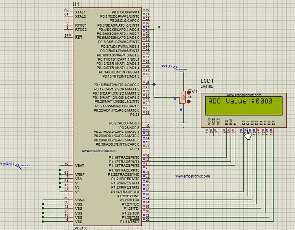 [ Please find the output image Here ]
|
|
|
That’s all guys… Now you can play around ADC. If you have any doubt please let us know. You can download this project from here.
In our next tutorial, we will see how to interface the LCD with LPC2148 (ARM7). If you want to use FreeRTOS on LPC2148, then please refer FreeRTOS series.
You can also read the below tutorials.
Embedded Software | Firmware | Linux Devic Deriver | RTOS
Hi, I am a tech blogger and an Embedded Engineer. I am always eager to learn and explore tech-related concepts. And also, I wanted to share my knowledge with everyone in a more straightforward way with easy practical examples. I strongly believe that learning by doing is more powerful than just learning by reading. I love to do experiments. If you want to help or support me on my journey, consider sharing my articles, or Buy me a Coffee! Thank you for reading my blog! Happy learning!
