This article is a continuation of the series of tutorials on the LPC2148 Microcontroller (ARM7). The aim of this series is to provide easy and practical examples that anyone can understand. In the previous tutorial, we have seen how to set up the PLL and clock for LPC2148 (ARM7). Now we are going to see LPC2148 GPIO Tutorial. Before that please read the Introduction of LPC2148.
Before going to GPIO Registers, We should know about the PINSEL register.
Table of Contents
LPC2148 GPIO Tutorial
PINSEL Register
A 32-bit register is used to select the function of the pins in which the user needs it to operate. As I said there are four functions for each pin of the controller, and the first function was GPIO ( General Purpose Input Output ). It means that the pin can either act as an Input or Output with no specific functions.
There are totally three PINSEL registers in LPC2148 Controller in order to control the functions of the Pins in the respective ports. The classification is given below
- PINSEL0 – Controls functions of Port0.0 – Port0.15
- PINSEL1 – Controls functions of Port0.16-Port0.31
- PINSEL2 – Controls functions of Port1.16-Port1.31
PINSEL0

|
|
|
PINSEL1

I/O PORT
LPC2141/2/4/6/8 has two 32-bit General Purpose I/O ports. A total of 30 input/output and a single output only pinout of 32 pins are available on PORT0. PORT1 has up to 16 pins available for GPIO functions. PORT0 and PORT1 are controlled via two groups of 4 registers.
Registers for GPIO
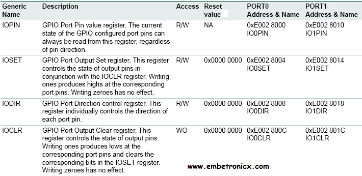
REGISTER DESCRIPTION
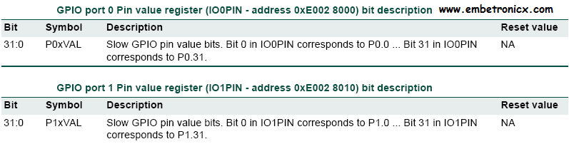
IOPIN
This register provides the value of port pins that are configured to perform only digital functions. The register will give the logic value of the pin regardless of whether the pin is configured for input or output, or as GPIO or an alternate digital function. As an example, a particular port pin may have GPIO input, GPIO output, UART receive, and PWM output as selectable functions. Any configuration of that pin will allow its current logic state to be read from the IOPIN register.
|
|
|
If a pin has an analog function as one of its options, the pin state cannot be read if the analog configuration is selected. Selecting the pin as an A/D input disconnects the digital features of the pin. In that case, the pin value read in the IOPIN register is not valid. Writing to the IOPIN register stores the value in the port output register, bypassing the need to use both the IOSET and IOCLR registers to obtain the entire written value. This feature should be used carefully in an application since it affects the entire port.
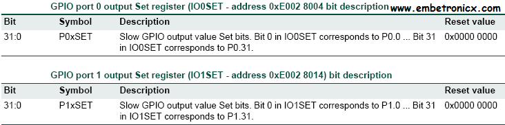
IOSET
This register is used to produce a HIGH level output at the port pins configured as GPIO in an OUTPUT mode. Writing 1 produces a HIGH level at the corresponding port pins. Writing 0 has no effect. If any pin is configured as an input or a secondary function, writing 1 to the corresponding bit in the IOSET has no effect. Reading the IOSET register returns the value of this register, as determined by previous writes to IOSET and IOCLR (or IOPIN as noted above). This value does not reflect the effect of any outside world influence on the I/O pins.
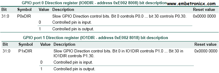
IODIR
This word accessible register is used to control the direction of the pins when they are configured as GPIO port pins. The direction bit for any pin must be set according to the pin functionality.
|
|
|
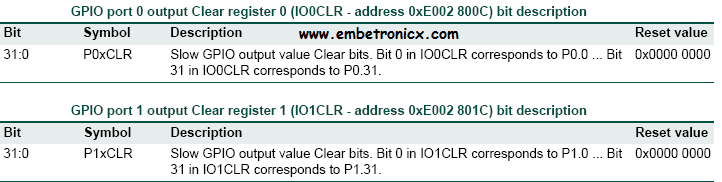
IOCLR
This register is used to produce a LOW-level output at port pins configured as GPIO in an OUTPUT mode. Writing 1 produces a LOW level at the corresponding port pin and clears the corresponding bit in the IOSET register. Writing 0 has no effect. If any pin is configured as an input or a secondary function, writing to IOCLR has no effect.
So this is the theory of LPC2148 GPIO. If you have any doubt about this please see the real-time example below. Then you will understand.
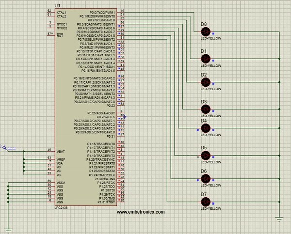
LED Interfacing – LPC2148 GPIO Tutorial
We already know about the LED and its operation. So we move to the program now. Go through the code below.
#include<lpc214x.h>

void delay();
void main()
{
    IO0DIR |=0XfffffFFF;              //Port 0 is now acting as a output pin
    while(1) {
        IOSET0 |=0XfffffFFF;      //Port 0's all pins are high now (LED is glowing)
        delay();
        IOCLR0 |=0XFFFfffff;      //Port 0's all pins are low now (LED is OFF)
        delay();
    }
}

void delay()
{
    unsigned int i;
    for(i=0;i<30000;i++);
}
OUTPUT
|
|
|
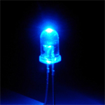
[ Please find the output image Here ]
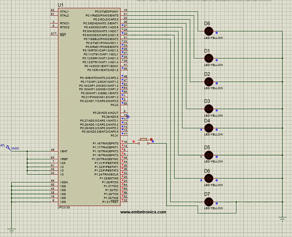
Switch Interfacing – LPC2148 GPIO Tutorial
#include<lpc214x.h>

void delay();
void main()
{
    IO0DIR |=0XfffffFFF;                   //Port 0 is now acting as a output pin
    IO1DIR = 0x0;                          //Port 1 is now acting as a input pin
    while(1)
    {
        if((IO1PIN & (1<<16)) ==0)     //Checking 16th pin of Port 1
            IOSET0 |=0XfffffFFF;   //Port 0's all pins are high now (LED is glowing)
        else
            IOCLR0 |=0XFFFfffff;   //Port 0's all pins are low now (LED is OFF)
    }

}

void delay()
{
    unsigned int i;
    for(i=0;i<30000;i++);
}
OUTPUT
 [ Please find the output image Here ]
TASKS
Here I’ve given some exercise for your practice. Please try that.
1. Blink alternate LEDs in Port1
2. Blink LEDs in a cyclic fashion
|
|
|
In our next tutorial, we will see LPC2148 Timer (ARM7) and configuration. If you want to use FreeRTOS on LPC2148, then please refer FreeRTOS series.
You can also read the below tutorials.
Embedded Software | Firmware | Linux Devic Deriver | RTOS
Hi, I am a tech blogger and an Embedded Engineer. I am always eager to learn and explore tech-related concepts. And also, I wanted to share my knowledge with everyone in a more straightforward way with easy practical examples. I strongly believe that learning by doing is more powerful than just learning by reading. I love to do experiments. If you want to help or support me on my journey, consider sharing my articles, or Buy me a Coffee! Thank you for reading my blog! Happy learning!
