Nowadays, wireless communication rules the entire world. There are many wireless communication technologies available like Bluetooth, Wifi, RF, etc. The NRF24L01 is one of the wireless transceiver RF modules used for SPI communication with a 2Mbps transmission speed. If you want to know or learn how the nRF24L01+ module works, then you are at the right place. In this article, we are going to only discuss the nRF24l01 wireless module (transceiver).
Before we start, we will tell you why it is really important to learn this nrf24l01 module. The main reason is it is very low cost. It is just around 2$. You can buy that here. Just buy that and use it in your projects.
Table of Contents
Hardware Overview of nRF24L01+ module
First, there are three modules available in the market. nRF24L01, nRF24L01+ and nRF24L01+ PA LNA.
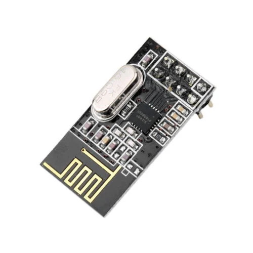 nRF24L01 RF Module nRF24L01 RF Module |
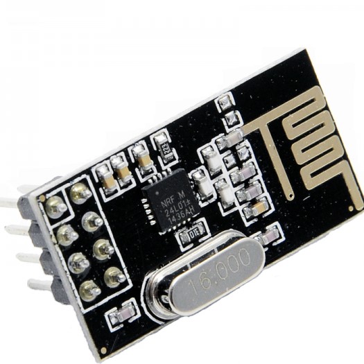 nRF24L01+ RF Module nRF24L01+ RF Module |
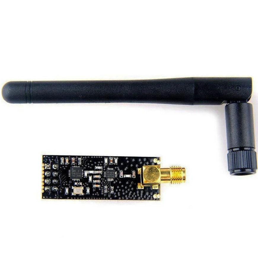 nRF24L01+ PA LNA RF Module nRF24L01+ PA LNA RF Module |
The main difference between the nRF24L01 and nRF24L01+ data rate. nRF24L01 has only 1Mbps and 2Mbps on-air data rate, while the nRF24L01+ version can also support 250Kbps. Both nRF24L01 and nRF24L01+ can be mixed together as long as 1MBps or 2 MBps is used as the data rate.
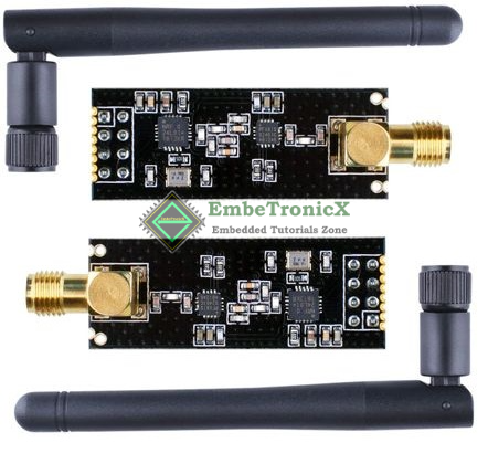
There are a few differences between nRF24L01+ and nRF24L01+ PA LNA that we will cover at the last. We will cover nRF24L01+ with PA LNA in this article.
|
|
|
nRF24L01+
nRF24L01+ is a single-chip 2.4GHz transceiver module used in data transmission. Each nRF24L01+ wireless transceiver module can send and receive data. Since it operates on the 2.4 GHz ISM band, the technology is approved for engineering applications in almost all countries. The data transfer rate is configurable and can be one of 250kbps, 1Mbps, and 2Mbps. Using the lower data rate gives a better receiver sensitivity than the higher data rate. But higher data rate consumes a lower average current and reduces the probability of on-air collisions.
The nRF24L01+ wireless transceiver module is powered by 3.3 Volts, so it can be easily used in both 3.2 Volts and 5 Volts systems.
For compatibility with nRF2401A, nRF24E1, nRF2402, and nRF24E2 the air data rate must be set to 250Kbps or 1Mbps.
nRF24L01+ Technical Specifications
The nRF24L01+ technical specifications and features are given below.
|
|
|
| Frequency Range | Worldwide 2.4 GHz ISM Band. |
| Channels | 126 Channels |
| Channel Spacing |
|
| Modulation | GFSK |
| Operating voltage | 1.9 V to 3.6 V |
| Data Rates | up to 2 Mbps (250Kbps, 1MBps, and 2Mbps) |
| Tx output power (Programmable) | 0dBm, -6dBm, -12dBm or -18dBm |
| Max Tx Operating Current | 11.3mA at 0dBm |
| Max Rx Operating Current | 12.3mA at 2Mbps |
| Operating Current(Standby Mode) | 22uA |
| Operating Current(Power Down Mode) | 900nA |
| Host Interface | 4-pin SPI up to 10Mbps |
For more details, please refer to the datasheet.
How does the nRF24L01+ Transceiver work?
nRF24L01+ operating modes
The nRF24L01+ has a built-in state machine that controls the transitions between the different operating modes of the chip. It has the below operating modes.
Power Down Mode
In the Power-down mode, nRF24L01+ will be disabled. So the power consumption will be minimal. In this mode, the SPI will be kept active and we can access the register values.
Standby Modes
These are the intermediate state before going for TX or RX mode. It has two modes called Standby Mode-I, and Standby Mode-II. Standby mode-I consumes less power because only the part of the crystal oscillator is active. In Standby mode-II, extra clock buffers are active. So, it will consume more power than Standby mode-I.
RX Mode
When we make the nRF24L01+ as a receiver, it will go to the RX mode. In this mode, the receiver continuously demodulates the signal from the RF channel and sends that to the baseband protocol engine. The baseband protocol engine checks whether the packet received is valid or not by checking the address and CRC. If that is a valid packet it will write that data to the RX FIFO. If the RX FIFO is full, then it will discard the data.
|
|
|
Note: nRF24L01+ wireless module remains in the RX mode until we configure it to go to Standby mode or Power-down mode. If the Enhanced ShockBurst feature is enabled, then it can enter to other modes.
TX Mode
When we transmit some data, the module will go to the TX mode. The nRF24L01+ wireless transceiver module will stay in the TX mode until it finishes the transmission of the current packet. After that, if the TX FIFO is empty, then it will go to Standby mode. If it is not empty, it will transmit the data in the TX FIFO until it becomes empty.
RF Channel Frequency
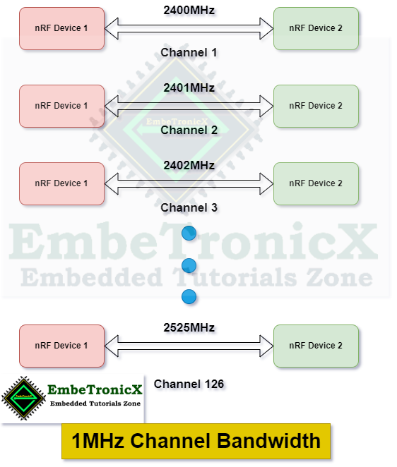
As we have already said, this nRF24L01+ wireless module communicates using the 2.4GHz ISM band. And the channel bandwidth is 1MHz at 1Mbps and 2MHz at 2Mbps. What does it mean?
Okay, we know the nRF24L01+ RF wireless module will communicate using 2400MHz (2.4GHz). If our channel bandwidth is 1MHz, then we can transmit or receive on 2400MHz, 22401MHz, 2402MHz, 2403MHz, 2404MHz … 2525MHz. For 2Mbps, we must use a channel bandwidth 2MHz or more to avoid non-overlapping channels. If we use 2MHz as channel bandwidth in 2Mbps, we can transmit and receive on 2400MHz, 2402MHz, 2404MHz, and so on.
For 1MHz channel bandwidth, we will have 126 channels and for 2MHz channel bandwidth, we have 63 channels.
|
|
|
A transmitter and a receiver must be programmed with the same RF channel frequency to be able to communicate with each other. If the channel bandwidth is 1MHz and the transmitter is transmitting using 2500MHz (channel 100), then the receiver must listen on the 100th channel (2500MHz). Then only it can be able to receive the data, otherwise, the data would be lost.
The below image will help you to understand more.
The RF channel frequency is set by the RF_CH register according to the following formula:
F0 = 2400 + RF_CH [MHz]
|
|
|
For example, if you select 100 as your channel for data transmission/reception, the RF channel frequency of your channel will be 2500 MHz (2400 + 100).
Enhanced ShockBurst™
Enhanced ShockBrust™ is a feature that is available in the nRF24L01+ RF wireless module. That will handle the below operations.
- Automatic packet handling
- Automatic packet assembly – Assembles the packet with a preamble, address, and other required information.
- Automatic packet validation – When the receiver receives the packet, it will check whether the packet is valid or not.
- Automatic packet disassembly – The valid received packet is disassembled and the payload is copied into the RX FIFO.
- Automatic acknowledgment – Automatically transmits an ACK to the transmitter after it has received the valid packet.
- Retransmissions of packets – If the ACK is not received from the receiver, then automatically the transmitter will retransmit the packet.
- 1 to 32 bytes dynamic payload length
- 6 data pipe Multiceiver™ for 1:6 star networks
nRF24L01+ Multiceiver
MultiCeiver is a feature that is implemented in this nRF24L01+ RF wireless module. It is nothing but a single receiver that can able to receive the data from multiple transmitters (up to 6) in a single frequency channel. So, already we have divided the frequency into 126 channels. Now, again we are dividing one channel into 6 pipes. This is implemented by using the 6 different parallel data pipes. Each data pipe has a unique address. The below diagram will help you to understand this.
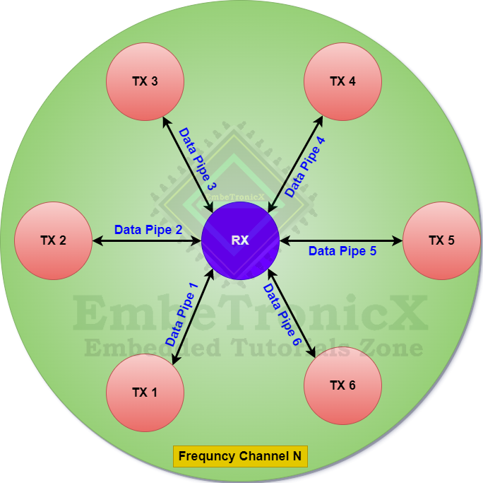
Only one data pipe in the receiver can receive the packet at a time. By default data pipe 0 and data pipe 1 are enabled. Others can be enabled by configuring the register. We can program the address of each data pipe and we should not use the same address for the data pipes.
|
|
|
nRF24L01+ Pinout
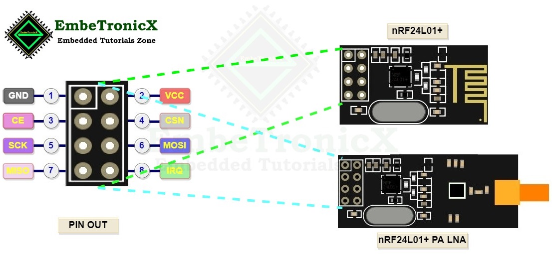
This nRF24L01+ RF radio has 8 pins.
- GND – Ground
- VCC – Input power to the RF radio. It can be anywhere from 1.9 to 3.9 volts. Remember if you give 5V to this pin, it may destroy your nRF24L01+ module.
- CE (Chip Enable) – This is used to activate the chip in RX or TX mode (Active High).
- CSN (Chip Select Not) – This will be kept high and when we want to send a command through SPI, we need to make this low. Every new command must be started by a high-to-low transition on this CSN pin.
- SCK (Serial Clock) – SPI clock.
- MOSI (Master Out Slave In) – SPI input to the nRF24L01.
- MISO (Master In Slave Out) – SPI output from the nRF24L01.
- IRQ – Interrupt pin that can alert the master when new data is available to process.
Controlling the nRF24L01+ RF wireless module
We can configure this nRF wireless module using the SPI communication from the Microcontroller. This nRF24L01+ module supports SPI up to 10Mbps. If you want to learn SPI, you can check out our SPI tutorial. In that article, we have explained SPI completely from the basics to the advanced.
We can configure and control the RF radio by accessing the register map using the SPI communication.
There are many 1-byte SPI commands available in this nRF24L01+. Using that commands, we can activate the nRF24L01+ wireless transceiver module data FIFO and access the registers of this RF wireless module.
|
|
|
First, we need to send the Command byte followed by the Data bytes.
Commands
As we said earlier there are many commands available for each operation. The commands are given below.
| COMMAND | COMMAND BYTE | OPERATION |
R_REGISTER |
000XXXXX |
This command is used to read the status registers. We have to replace XXXXX with the 5-bit register address. (1 – 5 bytes) |
W_REGISTER |
001XXXXX |
This command is used to write the data to the registers. We have to replace XXXXX with the 5-bit register address. This command can be executed in the Power down or standby modes.(1 – 5 bytes) |
R_RX_PAYLOAD |
01100001 |
This command is used to read RX-payload (1 – 32 bytes). The payload will be deleted from the FIFO after you read it. This is used in RX mode. |
W_TX_PAYLOAD |
10100000 |
Using this command we can write the payload (1– 32 bytes) to the TX FIFO. |
FLUSH_TX |
11100001 |
Using this command, we can flush the TX FIFO. This is used in the TX mode. |
FLUSH_RX |
11100010 |
Using this command, we can flush the RX FIFO. This is used in the RX mode. We should not execute this command while transmitting the acknowledge. |
REUSE_TX_PL |
11100011 |
This command will tell the RF radio to reuse the last payload. This will reuse the payload until we flush the TX FIFO using FLUSH_TX or write the new payload using the command W_TX_PAYLOAD. We should not activate or deactivate this command during the data transmission. |
R_RX_PL_WID |
01100000 |
Using this command we can read the RX payload width in the RX FIFO. We need to set the proper bits in the FEATURE register to use this feature. |
W_ACK_PAYLOAD |
10101PPP |
Write Payload to be transmitted together with ACK packet on PIPE PPP. (PPP is valid in the range from 000 to 101). A maximum of three ACK packet payloads can be pending. Payloads with the same PPP are handled using the first in – first out principle. Write payload: 1– 32 bytes. A write operation always starts at byte 0. We need to set the proper bits in the FEATURE register to use this feature. |
W_TX_PAYLOAD_NOACK |
10110000 |
This is used in TX mode. Disables AUTOACK on this specific packet. We need to set the proper bits in the FEATURE register to use this feature. |
NOP |
11111111 |
No Operation. Might be used to read the STATUS register. |
Register Map
In our previous section, we have seen the commands that are used to access the nRF24L01+ registers. In this section, we will see all the registers. We can control the RF radio by accessing the below registers using the above SPI commands.
CONFIG Register
This register is used to configure the radio. The address of this CONFIG register is 0x00.
| Bit 7 | Bit 6 | Bit 5 | Bit 4 | Bit 3 | Bit 2 | Bit 1 | Bit 0 |
Reserved |
MASK_RX_DR |
MASK_TX_DS |
MASK_MAX_RT |
EN_CRC |
CRCO |
PWR_UP |
PRIM_RX |
Reserved– Reserved bit. Only 0 is allowed.MASK_RX_DR– Mask interrupt caused byRX_DR1 – Don’t generate the interrupt in the IRQ pin, 0 – Generate the active low interrupt on the IRQ pin.MASK_TX_DS– Mask interrupt caused byTX_DS1 – Don’t generate the interrupt in the IRQ pin, 0 – Generate the active low interrupt on the IRQ pin.MASK_MAX_RT– Mask interrupt caused byMAX_RT1 – Don’t generate the interrupt in the IRQ pin, 0 – Generate the active low interrupt on the IRQ pin.EN_CRC– If we set this bit, it will enable the CRC check. This will be forced high if one of the bits in theEN_AAis high.CRCO– This will configure the CRC encoding scheme. ‘0‘ – 1 byte, ‘1‘ – 2 bytes.PWR_UP– ‘1‘ – Power Up, ‘0‘ – Power DownPRIM_RX– Rx/Tx control. ‘1‘ – PRX, ‘0‘ – PTX.
EN_AA Register
This register is used to enable the auto acknowledgment functionality in the radio. The address of this EN_AA register is 0x01.
|
|
|
| Bit 7 | Bit 6 | Bit 5 | Bit 4 | Bit 3 | Bit 2 | Bit 1 | Bit 0 |
Reserved |
Reserved |
ENAA_P5 |
ENAA_P4 |
ENAA_P3 |
ENAA_P2 |
ENAA_P1 |
ENAA_P0 |
Reserved– Reserved bit. Only 0 is allowed.ENAA_P5– Enable auto acknowledgment data pipe 5ENAA_P4– Enable auto acknowledgment data pipe 4ENAA_P3– Enable auto acknowledgment data pipe 3ENAA_P2– Enable auto acknowledgment data pipe 2ENAA_P1– Enable auto acknowledgment data pipe 1ENAA_P0– Enable auto acknowledgment data pipe 0
EN_RXADDR Register
This EN_RXADDR enables the RX addresses. The address of this register is 0x02.
| Bit 7 | Bit 6 | Bit 5 | Bit 4 | Bit 3 | Bit 2 | Bit 1 | Bit 0 |
Reserved |
Reserved |
ERX_P5 |
ERX_P4 |
ERX_P3 |
ERX_P2 |
ERX_P1 |
ERX_P0 |
Reserved– Reserved bit. Only 0 is allowed.ENAA_P5– Enable data pipe 5ENAA_P4– Enable data pipe 4ENAA_P3– Enable data pipe 3ENAA_P2– Enable data pipe 2ENAA_P1– Enable data pipe 1ENAA_P0– Enable data pipe 0
SETUP_AW Register
This SETUP_AW register is used to set up the address width of all data pipes. The address of this register is 0x03.
| Bit 7 | Bit 6 | Bit 5 | Bit 4 | Bit 3 | Bit 2 | Bit 1 | Bit 0 |
Reserved |
Reserved |
Reserved |
Reserved |
Reserved |
Reserved |
AW:1 |
AW:0 |
Reserved– Reserved bit. Only 0 is allowed.AW:1 AW:0– ‘00‘ Not allowed, ‘01‘ – 3 bytes, ‘10‘ – 4 bytes, ‘11‘ – 5 bytes.
SETUP_RETR Register
This register is used to set up the Automatic retransmission. The address of this register is 0x04.
| Bit 7 | Bit 6 | Bit 5 | Bit 4 | Bit 3 | Bit 2 | Bit 1 | Bit 0 |
ARD:3 |
ARD:2 |
ARD:1 |
ARD:0 |
ARC:3 |
ARC:2 |
ARC:1 |
ARC:0 |
ARD:3 ARD:0– Auto retransmit delay. ‘0000‘ – 250us, ‘0001‘ – 500us, ‘0010‘ – 750us, … ‘1111‘ – 4000us.ARC:3 ARC:0– Auto retransmit count. ‘0000‘ – disabled, ‘0001‘ – 1 retry, ‘0010‘ – 2 retry, … ‘1111‘ – 15 retry.
RF_CH Register
This register is used to set up the RF channel. The address of this register is 0x05.
| Bit 7 | Bit 6 | Bit 5 | Bit 4 | Bit 3 | Bit 2 | Bit 1 | Bit 0 |
Reserved |
RF_CH:6 |
RF_CH:5 |
RF_CH:4 |
RF_CH:3 |
RF_CH:2 |
RF_CH:1 |
RF_CH:0 |
Reserved– Reserved bit. Only 0 is allowed.- RF_CH:6 RF_CH:0 – Sets the frequency channel. ‘0000000‘ – channel 0, ‘0000001‘ – Channel 1, till channel 125.
RF_SETUP Register
This RF_SETUP register is used to set up the RF. The address of this register is 0x06.
|
|
|
| Bit 7 | Bit 6 | Bit 5 | Bit 4 | Bit 3 | Bit 2 | Bit 1 | Bit 0 |
CONT_WAVE |
Reserved |
RF_DR_LOW |
PLL_LOCK |
RF_DR_HIGH |
RF_PWR:1 |
RF_PWR:0 |
Obsolete |
CONT_WAVE– Enables continuous carrier transit when high.Reserved– Reserved bit. Only 0 is allowed.RF_DR_LOW– Sets RF data rate to 250Kbps.PLL_LOCK– Force PLL lock signal( used only for testing).RF_DR_HIGH– Sets high-speed RF data rates. ‘0‘ – 1Mbps, ‘1’ – 2Mbps. If theRF_DR_LOWbit is set, then this bit will be don’t care.- RF_PWR:1 RF_PWR:0 – SetRF output power. ‘00‘ : -18dBm, ‘01‘ : -12dBm, ‘10‘ : -6dBm, ‘11‘ : 0dBm
Obsolete– Don’t care
STATUS Register
This is the status register and its address is 0x07.
| Bit 7 | Bit 6 | Bit 5 | Bit 4 | Bit 3 | Bit 2 | Bit 1 | Bit 0 |
Reserved |
RX_DR |
TX_DS |
MAX_RT |
RX_P_NO:2 |
RX_P_NO:1 |
RX_P_NO:0 |
TX_FULL |
Reserved– Reserved bit. Only 0 is allowed.RX_DR– Data Ready RX FIFO interrupt. Asserted when new data arrives RX FIFO. Write 1 to clear bit.TX_DS– Data Sent TX FIFO interrupt. Asserted when packet transmitted on TX. IfAUTO_ACKis activated, this bit is set high only when ACK is received. Write 1 to clear bit.MAX_RT– Maximum number of TX retransmits interrupt Write 1 to clear bit. If MAX_RT is asserted it must be cleared to enable further communication.RX_P_NO:2 RX_P_NO:0TX_FULL– TX FIFO Full flag. ‘1‘- TXFIFO Full, ‘0‘- One or more TX FIFO is free.
OBSERVE_TX Register
This OBSERVE_TX register is used to transmit the observe register. The address of this register is 0x08.
| Bit 7 | Bit 6 | Bit 5 | Bit 4 | Bit 3 | Bit 2 | Bit 1 | Bit 0 |
PLOS_CNT:3 |
PLOS_CNT:2 |
PLOS_CNT:1 |
PLOS_CNT:0 |
ARC_CNT:3 |
ARC_CNT:2 |
ARC_CNT:1 |
ARC_CNT:0 |
PLOS_CNT:3 PLOS_CNT:0– This has the count of the lost packets. This is overflow protected. So, when it reaches count 15, it will discontinue the transmission until reset. We can reset this count by writing theRF_CHregister.ARC_CNT:3 ARC_CNT:0– Retransmitted packet count. This will be reset once the new packet starts.
CD Register
This CD register is used to enable the carrier detect. The address of this register is 0x09.
| Bit 7 | Bit 6 | Bit 5 | Bit 4 | Bit 3 | Bit 2 | Bit 1 | Bit 0 |
Reserved |
Reserved |
Reserved |
Reserved |
Reserved |
Reserved |
Reserved |
CD |
Reserved– Reserved bit. Only 0 is allowed.CD– Enables carrier detection.
RX_ADDR_P0 Register
5 bytes register which is used to set the address for the data pipe 0 for RX operation. The address of this register is 0x0A.
RX_ADDR_P1 Register
5 bytes register which is used to set the address for the data pipe 1 for RX operation. The address of this register is 0x0B.
|
|
|
RX_ADDR_P2 Register
1-byte register which is used to set the address for the data pipe 2 for RX operation. This is only LSB. Another 4 bytes will be used from the RX_ADDR_P0 register. The address of this register is 0x0C.
RX_ADDR_P3 Register
1-byte register which is used to set the address for the data pipe 3 for RX operation. This is only LSB. Another 4 bytes will be used from the RX_ADDR_P0 register. The address of this register is 0x0D.
RX_ADDR_P4 Register
1-byte register which is used to set the address for the data pipe 4 for RX operation. This is only LSB. Another 4 bytes will be used from the RX_ADDR_P0 register. The address of this register is 0x0E.
RX_ADDR_P5 Register
1-byte register which is used to set the address for the data pipe 5 for RX operation. This is only LSB. Another 4 bytes will be used from the RX_ADDR_P0 register. The address of this register is 0x0F.
TX_ADDR Register
5 bytes register which is used to set the address for the TX operation. The address of this register is 0x10.
|
|
|
RX_PW_P0 Register
This register will have the number of bytes in the RX payload in data pipe 0. The address of this register is 0x11.
| Bit 7 | Bit 6 | Bit 5 | Bit 4 | Bit 3 | Bit 2 | Bit 1 | Bit 0 |
Reserved |
Reserved |
RX_PW_P0:5 |
RX_PW_P0:4 |
RX_PW_P0:3 |
RX_PW_P0:2 |
RX_PW_P0:1 |
RX_PW_P0:0 |
Reserved– Reserved bit. Only 0 is allowed.RX_PW_P0:5 RX_PW_P0:0
RX_PW_P1 Register
This register will have the number of bytes in the RX payload in data pipe 1. The address of this register is 0x12.
| Bit 7 | Bit 6 | Bit 5 | Bit 4 | Bit 3 | Bit 2 | Bit 1 | Bit 0 |
Reserved |
Reserved |
RX_PW_P1:5 |
RX_PW_P1:4 |
RX_PW_P1:3 |
RX_PW_P1:2 |
RX_PW_P1:1 |
RX_PW_P1:0 |
Reserved– Reserved bit. Only 0 is allowed.RX_PW_P1:5 RX_PW_P1:0– Number of bytes in RX payload in data pipe 1. 0 = Disabled, 1 = 1byte, 2 = 2bytes … 32 = 32 bytes.
RX_PW_P2 Register
This register will have the number of bytes in the RX payload in data pipe 2. The address of this register is 0x13.
| Bit 7 | Bit 6 | Bit 5 | Bit 4 | Bit 3 | Bit 2 | Bit 1 | Bit 0 |
Reserved |
Reserved |
RX_PW_P2:5 |
RX_PW_P2:4 |
RX_PW_P2:3 |
RX_PW_P2:2 |
RX_PW_P2:1 |
RX_PW_P2:0 |
Reserved– Reserved bit. Only 0 is allowed.RX_PW_P2:5 RX_PW_P2:0– Number of bytes in RX payload in data pipe 2. 0 = Disabled, 1 = 1byte, 2 = 2bytes … 32 = 32 bytes.
RX_PW_P3 Register
This register will have the number of bytes in the RX payload in data pipe 3. The address of this register is 0x14.
| Bit 7 | Bit 6 | Bit 5 | Bit 4 | Bit 3 | Bit 2 | Bit 1 | Bit 0 |
Reserved |
Reserved |
RX_PW_P3:5 |
RX_PW_P3:4 |
RX_PW_P3:3 |
RX_PW_P3:2 |
RX_PW_P3:1 |
RX_PW_P3:0 |
Reserved– Reserved bit. Only 0 is allowed.RX_PW_P3:5 RX_PW_P3:0– Number of bytes in RX payload in data pipe 3. 0 = Disabled, 1 = 1byte, 2 = 2bytes … 32 = 32 bytes.
RX_PW_P4 Register
This register will have the number of bytes in the RX payload in data pipe 4. The address of this register is 0x15.
|
|
|
| Bit 7 | Bit 6 | Bit 5 | Bit 4 | Bit 3 | Bit 2 | Bit 1 | Bit 0 |
Reserved |
Reserved |
RX_PW_P4:5 |
RX_PW_P4:4 |
RX_PW_P4:3 |
RX_PW_P4:2 |
RX_PW_P4:1 |
RX_PW_P4:0 |
Reserved– Reserved bit. Only 0 is allowed.RX_PW_P4:5 RX_PW_P4:0– Number of bytes in RX payload in data pipe 4. 0 = Disabled, 1 = 1byte, 2 = 2bytes … 32 = 32 bytes.
RX_PW_P5 Register
This register will have the number of bytes in the RX payload in data pipe 5. The address of this register is 0x16.
| Bit 7 | Bit 6 | Bit 5 | Bit 4 | Bit 3 | Bit 2 | Bit 1 | Bit 0 |
Reserved |
Reserved |
RX_PW_P5:5 |
RX_PW_P5:4 |
RX_PW_P5:3 |
RX_PW_P5:2 |
RX_PW_P5:1 |
RX_PW_P5:0 |
Reserved– Reserved bit. Only 0 is allowed.RX_PW_P5:5 RX_PW_P5:0– Number of bytes in RX payload in data pipe 5. 0 = Disabled, 1 = 1byte, 2 = 2bytes … 32 = 32 bytes.
FIFO_STATUS Register
This register is used to read the FIFO status. The address of this register is 0x17.
| Bit 7 | Bit 6 | Bit 5 | Bit 4 | Bit 3 | Bit 2 | Bit 1 | Bit 0 |
Reserved |
TX_REUSE |
TX_FULL |
TX_EMPTY |
Reserved |
Reserved |
RX_FULL |
RX_EMPTY |
Reserved– Reserved bit. Only 0 is allowed.TX_REUSE– If we set this bit, it will reuse the last transmitted payload. The packet will be retransmitted as long as CE is high.TX_FULL– If this bit is set the TX FIFO is full. Otherwise, FIFO is not full.TX_EMPTY– If this bit is set the TX FIFO is empty. Otherwise, FIFO is not empty.Reserved– Reserved bit. Only 0 is allowed.RX_FULL–If this bit is set the RX FIFO is full. Otherwise, FIFO is not full.RX_EMPTY– If this bit is set the RX FIFO is empty. Otherwise, FIFO is not empty.
Note: Register addresses 0x18 to 0x1B are reserved for test purposes, altering them will make the chip malfunction.
DYNPD Register
This DYNPD register is used to enable the dynamic payload length. This register address is 0x1C.
| Bit 7 | Bit 6 | Bit 5 | Bit 4 | Bit 3 | Bit 2 | Bit 1 | Bit 0 |
Reserved |
Reserved |
DPL_P5 |
DPL_P4 |
DPL_P3 |
DPL_P2 |
DPL_P1 |
DPL_P0 |
Reserved– Reserved bit. Only 0 is allowed.DPL_P5– Enable dynamic payload length data pipe 5. (RequiresEN_DPLandENAA_P5)DPL_P4– Enable dynamic payload length data pipe 4. (RequiresEN_DPLandENAA_P4)DPL_P3– Enable dynamic payload length data pipe 3. (RequiresEN_DPLandENAA_P3)DPL_P2– Enable dynamic payload length data pipe 2. (RequiresEN_DPLandENAA_P2)DPL_P1– Enable dynamic payload length data pipe 1. (RequiresEN_DPLandENAA_P1)DPL_P0– Enable dynamic payload length data pipe 0. (RequiresEN_DPLandENAA_P0)
FEATURE Register
This DYNPD register is used to enable the dynamic payload length. This register address is 0x1C.
|
|
|
| Bit 7 | Bit 6 | Bit 5 | Bit 4 | Bit 3 | Bit 2 | Bit 1 | Bit 0 |
Reserved |
Reserved |
Reserved |
Reserved |
Reserved |
EN_DPL |
EN_ACK_PAY |
DPL_EN_DYN_ACK |
Reserved– Reserved bit. Only 0 is allowed.EN_DPL– Enable dynamic payload length.EN_ACK_PAY– Enable payload with ACK.DPL_EN_DYN_ACK– Enables theW_TX_PAYLOAD_NOACKcommand.
Okay, yes this is a very long story. It has these many registers in the nRF24L01+ RF wireless module.
Applications of nRF24L01+ Wireless Transceiver Module
- Wireless PC Peripherals
- Mouse, keyboards, and remotes
- 3-in-one desktop bundles
- Advanced Media center remote controls
- VoIP headsets
- Game controllers
- Sports watches and sensors
- RF remote controls for consumer electronics
- Home and commercial automation
- Ultra-low power sensor networks
- Active RFID
- Asset tracing systems
- Toys
Differences between nRF24L01+ and nRF24L01+ PA LNA
| nRF24L01+ | nRF24L01+ PA LNA |
|
|
| This has an onboard antenna. | It comes with an external IPX antenna. |
| It doesn’t have PA (Power Amplifier) and LNA (Low-Noise Amplifier). | It has PA (Power Amplifier) and LNA (Low-Noise Amplifier). |
| In open space, it covers a distance of 100 meters. | In open space, it covers a distance of 1000 meters. |
What is PA and LNA?
A power Amplifier amplifies the signal strength being transmitted from the nRF24L01+ rf module and a Low-Noise Amplifier takes an extremely weak signal from the antenna and amplifies it to a more useful level. The LNA is used in the receive path and the PA is used in the transmit path.
We have used the nRF24L01 module in our projects. You can refer to that.
- nRF24L01 interfacing with 8051
- nRF24L01 interfacing with ESP32
- nRF24L01 interfacing with STM32
- nRF24L01 interfacing with Raspberry Pi Pico
You can also read the below tutorials.
|
|
|
Embedded Software | Firmware | Linux Devic Deriver | RTOS
Hi, I am a tech blogger and an Embedded Engineer. I am always eager to learn and explore tech-related concepts. And also, I wanted to share my knowledge with everyone in a more straightforward way with easy practical examples. I strongly believe that learning by doing is more powerful than just learning by reading. I love to do experiments. If you want to help or support me on my journey, consider sharing my articles, or Buy me a Coffee! Thank you for reading my blog! Happy learning!
