In our previous tutorial, we have seen a gas detection sensor interfacing with 8051. NRF24L01 interfacing with 8051 tutorial is intended to enable wireless data transfer for 8051. So to do that, we will interface nRF24L10 with 8051. This will enable us to transfer the data wirelessly (by air) between two 8051 boards using NRF24L01.
Table of Contents
NRF24L01 interfacing with 8051
Hardware Required
- 8051 Development board – 2
- NRF24L01 – 2
- PC (To send/read data through UART using any serial terminal)
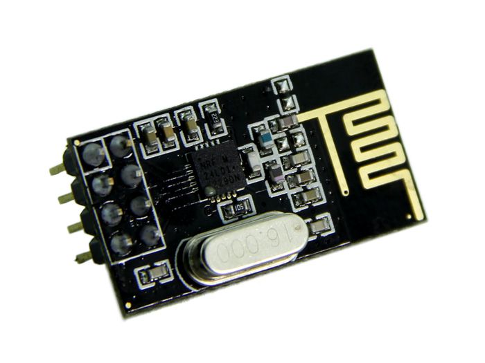
NRF24L0
Before start coding, we will see something about NRF24L01 to get some idea.
The nRF24L01 is a wireless transceiver module, meaning each module can both send as well as receive data. They operate at the frequency of 2.4GHz, which falls under the ISM band, and hence it is legal to use in almost all countries for engineering applications. The modules when operated efficiently can cover a distance of 100 meters (200 feet) which makes it a great choice for all wireless remote-controlled projects.
The module operates at 3.3V hence can be easily used with 3.2V systems or 5V systems. Each module has an address range of 125 and each module can communicate with 6 other modules hence it is possible to have multiple wireless units communicating with each other in a particular area. Hence mesh networks or other types of networks are possible using this module. So if you are looking for a wireless module with the above properties then this module would be an ideal choice for you.
|
|
|
These modules are very cheap, smaller in size, and have a lot of specifications. Some of the specifications of these modules are as follows,
nRF24L01 Features
- 2.4GHz RF transceiver Module
- Operating Voltage: 3.3V
- Nominal current: 50mA
- Range: 50 – 200 feet
- Operating current: 250mA (maximum)
- Communication Protocol: SPI
- Baud Rate: 250 kbps – 2 Mbps.
- Channel Range: 125
- Maximum Pipelines/node: 6
- Low-cost wireless solution
Note: Complete Technical Details can be found on the NRF24L01 datasheet.
nRF24L01 Pin Configuration
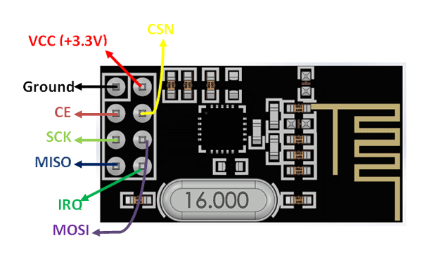
| Pin Number | Pin Name | Abbreviation | Function |
| 1 | Ground | Ground | Connected to the Ground of the system |
| 2 | Vcc | Power | Powers the module using 3.3V |
| 3 | CE | Chip Enable | Used to enable SPI communication |
| 4 | CSN | Ship Select Not | This pin has to be kept high always, else it will disable the SPI |
| 5 | SCK | Serial Clock | Provides the clock pulse using which the SPI communication works |
| 6 | MOSI | Master Out Slave In | Connected to MOSI pin of MCU, for the module to receive data from the MCU |
| 7 | MISO | Master In Slave Out | Connected to MISO pin of MCU, for the module to send data from the MCU |
| 8 | IRQ | Interrupt | It is an active low pin and is used only if the interrupt is required |
Applications
- Wireless Control application
- Mesh Networks
- RF Remote Controllers
- Connected devices
How to Use the NRF24L01
The NRF24L01 module works with the help of SPI communications. These modules can either be used with a 3.3V microcontroller or a 5V microcontroller but they should have an SPI port. Since 8051 doesn’t have the SPI, we are going to implement the SPI using the bit-banging method.
And SPI will be having just 4 lines but here it has one more line extra called CE pin to enable reception, transmission, and put the device into standby mode.
|
|
|
Write Register
- Write SPI write register address + 0x20
- Then write register value
Read Register
- Write the registered address
- Read the data
One status register is there (0x07). You can read the status of the transaction.
For more information, please check the datasheet.
Programming – NRF24L01 interfacing with 8051
In this tutorial, we are going to use one setup for transmitter purpose and another for receiver purpose. The concept is much simple. When we send something through the serial port in the transmitter, that will be transmitted over the air. Since we are using the same address for both TX and RX, RX will receive the data from the air and print the data through the serial port.
You can get the complete source code from GitHub.
Connection
- MISO – Port 1.0
- MOSI – Port 1.1
- SCK – Port 1.2
- CSN – Port 1.3
- CE – Port 1.4
TX Code
We have added only the NRF24L01 related source code. You can get the full project’s code from GitHub.
|
|
|
nRF24L01.h
#include<intrins.h>
#include<reg51.h>
#include"SERIAL.H"

#define TX_mode                      //If u want to receive Change to RX_mode

sbit MISO = P1^0;                    //SPI signal
sbit MOSI = P1^1;                    //SPI signal
sbit SCK  = P1^2;                    //SPI signal-Clk
sbit CSN  = P1^3;                    //SPI signal-Chip select
sbit CE   = P1^4;                    //this signal is active high and is used to activate the chip in RX or TX mode

//Commands
#define  R_REG       0x00            //Read command from reg
#define W_REG        0x20            //Write command to reg
#define R_RX_PL      0x61            //RX payload register address
#define W_TX_PL      0xA0            //TX payload register address
#define FLUSH_TX     0xE1            //Flush TX register
#define FLUSH_RX     0xE2            //Flush RX register
#define REUSE_TX_PL  0xE3            //Reuse TX payload register
#define NOP          0xFF            //No operation, might be used to read status register

//Register Address
#define CONFIG       0x00            //'Config' Reg
#define EN_AA        0x01            //Enable Auto Ack Reg
#define EN_RXADDR    0x02            //Enabled RX Addresses Reg
#define SETUP_AW     0x03            //Setup of Address Widths Reg
#define SETUP_PETR   0x04            //Setup of Automatic Retransmission Reg
#define RF_CH        0x05            //RF Channel Reg
#define RF_SETUP     0x06            //RF Setup Reg
#define STATUS       0x07            //Status Reg
#define OBSERVE_TX   0x08            //Transmit observe Reg
#define CD           0x09            //Carrier Detect Reg
#define RX_ADDR_P0   0x0A            //Receive address data pipe 0
#define RX_ADDR_P1   0x0B            //Receive address data pipe 1
#define RX_ADDR_P2   0x0C            //Receive address data pipe 2
#define RX_ADDR_P3   0x0D            //Receive address data pipe 3
#define RX_ADDR_P4   0x0E            //Receive address data pipe 4
#define RX_ADDR_P5   0x0F            //Receive address data pipe 5
#define TX_ADDR      0x10            //Transmit address. Used for a PTX device only
#define RX_PW_P0     0x11            //RX payload width, pipe 0
#define RX_PW_P1     0x12            //RX payload width, pipe 1
#define RX_PW_P2     0x13            //RX payload width, pipe 2
#define RX_PW_P3     0x14            //RX payload width, pipe 3
#define RX_PW_P4     0x15            //RX payload width, pipe 4
#define RX_PW_P5     0x16            //RX payload width, pipe 5
#define FIFO_STATUS  0x17            //FIFO Status Reg

#define TX_PLOAD_WIDTH 1
#define TX_ADD_WIDTH   5

const unsigned char TX_ADDRESS[TX_ADD_WIDTH] ={'i','n','t','e','r'};
unsigned char read_buf[TX_PLOAD_WIDTH+1];

volatile unsigned char bdata ack;
sbit RX_DR=ack^6;
sbit TX_DS=ack^5;
sbit MAX_RT=ack^4;

volatile unsigned char bdata buffer;
sbit msb = buffer^7;
sbit lsb = buffer^0;

void spi_delay(void);                                                                 //Delay
void nRF_config(void);                                                                //Select RX or TX
unsigned char spi_W(unsigned char);                                                   //Write byte and read the status
unsigned char spi_WREG(unsigned char,unsigned char);                                  //Write byte to REG and Read Status
unsigned char spi_WBUF(unsigned char reg,unsigned char *buff ,unsigned char count);   //Write the no of char to REG
unsigned char spi_RREG(unsigned char);                                                //Read the REG that have one byte
void spi_RBUF(unsigned char reg,unsigned char count);                                 //Read the REG that have more than one byte

unsigned char TX_PL(const unsigned char *payload);                                    //Transmit payload
unsigned char* RX_PL(void);                                                           //Receive payload

void get_status(void);                                                                //Get the status
void clear_irq(void);                                                                 //Clear IRQ bits (TX_DS, MAX_RT, RX_DR)

void spi_delay()
{
  _nop_();_nop_();_nop_();_nop_();_nop_();_nop_();_nop_();
  _nop_();_nop_();_nop_();_nop_();_nop_();_nop_();_nop_();
}

void get_status(void)
{
  ack=0;
  ack=spi_RREG(STATUS);
}

void clear_irq()
{
  spi_WREG(W_REG|STATUS,0x70);              //Clear RX_DR, TX_DS, MAX_RT flags
}

void nRF_config()
{
  CE=0;                             //Chip enable
  CSN=1;                            //SPI disable
  SCK=0;                            //SPI clock line init high


#ifdef TX_mode
  spi_WBUF(W_REG|TX_ADDR,TX_ADDRESS,TX_ADD_WIDTH);      //Set static TX address
  spi_WBUF(W_REG|RX_ADDR_P0,TX_ADDRESS,TX_ADD_WIDTH);   //Set static RX address for auto ack
#endif

#ifdef RX_mode
  CE=0;
  spi_WREG(FLUSH_RX,NOP);                                 //Clear the RX_FIFO
  spi_WREG(W_REG|CONFIG,0x0F);                            //Set PWR_UP bit, enable CRC(2 bytes) & Prim:RX. RX_DR enabled
  spi_WREG(W_REG|EN_AA,0x01);                             //Enable ShockBurst (Enable Auto ACK)
  spi_WREG(W_REG|SETUP_AW,0x03);                          //Puts the address field width 5bytes
  spi_WREG(W_REG|RF_CH,0x6E);                             //Set frequency channel 110 (2.510MHz)
  spi_WREG(W_REG|RF_SETUP,0x06);                          //Setup: 1Mbps, 0dBm, LNA off
  spi_WREG(W_REG|EN_RXADDR,0x01);                         //Enable data pipe 0
  spi_WBUF(W_REG|RX_ADDR_P0,TX_ADDRESS,TX_ADD_WIDTH);     //Set static RX address
  spi_WREG(W_REG|RX_PW_P0,TX_PLOAD_WIDTH);                //Set RX payload length
  CE=1;
#endif
}

unsigned char spi_W(unsigned char buf)
{
  int sp;
  buffer=buf;
  for(sp=0;sp<=7;sp++)
  {
    MOSI=msb;                     //MSB to MOSI-OUTPUT
    buffer=buffer<<1;
    SCK=1;
    buffer&=0xfe;                //Clear 0th bit
    buffer|=MISO;                //capture current MISO bit
    SCK=0;
  }
  return buffer;
}

unsigned char spi_WREG(unsigned char reg,unsigned char value)
{
  unsigned char stat;
  CSN=0;                      //CSN low, init SPI transaction
  stat=spi_W(reg);            //Select Reg
  spi_W(value);               //Send Value
  CSN=1;                      //CSN high
  return stat;
}

unsigned char spi_WBUF(unsigned char reg,unsigned char *buff ,unsigned char count)
{
  unsigned char stat,sp;
  CSN=0;
  stat=spi_W(reg);
  for(sp=0;sp<count;sp++)
  {
    spi_W(buff[sp]);
  }
  CSN=1;
  return stat;
}

#ifdef TX_mode
unsigned char TX_PL(unsigned char *payload)
{
  unsigned char stat;
  clear_irq();
  CE=0;
  spi_WREG(FLUSH_TX,NOP);                    //Clear the TX_FIFO
  spi_WREG(W_REG|CONFIG,0x00);               //PRIM_RX : PTX
  spi_WREG(W_REG|EN_AA,0x01);                //Enable ShockBurst (Enable Auto ACK)
  spi_WREG(W_REG|EN_RXADDR,0x01);            //Enable data pipe 0
  spi_WREG(W_REG|SETUP_AW,0x03);             // Puts the address field width 5bytes
  spi_WREG(W_REG|SETUP_PETR,0x1A);           //Auto retransmit: wait 500us, 10 retries
  spi_WREG(W_REG|RF_CH,0x6E);                //Set frequency channel 110 (2.510MHz)
  spi_WREG(W_REG|RF_SETUP,0x06);             //Setup: 1Mbps, 0dBm, LNA off
  spi_WREG(W_REG|CONFIG,0x0E);               //Set PWR_UP bit, enable CRC(2 bytes) & Prim:TX. MAX_RT & TX_DS enabled
  spi_WBUF(W_TX_PL,payload,TX_PLOAD_WIDTH);  //Write specified buffer to FIFO

  CE=1;
  spi_delay();
  CE=0;
  get_status();
  if(MAX_RT)
    return 0;
  if(TX_DS)
    return 1;
  return stat;
}
#endif

unsigned char spi_RREG(unsigned char reg)
{
  unsigned char rd;
  CSN=0;
  spi_W(reg);
  rd=spi_W(0);
  CSN=1;
  return rd;
}

#ifdef RX_mode
void spi_RBUF(unsigned char reg,unsigned char count)
{
  unsigned char stat,sp;
  CSN = 0;                        // Set CSN low, init SPI tranaction
  stat=spi_W(reg);
  for(sp=0;sp<count;sp++)
  {
    read_buf[sp]=spi_W(0);
  }
  read_buf[sp]='\0';
  CSN = 1;                        // Set CSN high again
}


unsigned char* RX_PL()
{
  spi_WREG(FLUSH_RX,NOP);
  do
  {
    get_status();
  }while(RX_DR==0);
  if(RX_DR)
  {
    clear_irq();
    get_status();
    if(ack ==0)
    {
      spi_RBUF(R_RX_PL,TX_PLOAD_WIDTH);
      spi_delay();
      return read_buf;
    }
  }
}
#endif
RX Code
We have added only the NRF24L01 related source code. You can get the full project’s code from GitHub.
nRF24L01.h
#include<intrins.h>
#include<reg51.h>
#include"SERIAL.H"

#define RX_mode                      //If u want to receive Change to RX_mode

sbit MISO = P1^0;                   //SPI signal
sbit MOSI = P1^1;                    //SPI signal
sbit SCK  = P1^2;                    //SPI signal-Clk
sbit CSN  = P1^3;                    //SPI signal-Chip select
sbit CE   = P1^4;                    //this signal is active high and is used to activate the chip in RX or TX mode

//Commands
#define  R_REG       0x00            //Read command from reg
#define W_REG        0x20            //Write command to reg
#define R_RX_PL      0x61            //RX payload register address
#define W_TX_PL      0xA0            //TX payload register address
#define FLUSH_TX     0xE1            //Flush TX register
#define FLUSH_RX     0xE2            //Flush RX register
#define REUSE_TX_PL  0xE3            //Reuse TX payload register
#define NOP          0xFF            //No operation, might be used to read status register

//Register Address
#define CONFIG       0x00            //'Config' Reg
#define EN_AA        0x01            //Enable Auto Ack Reg
#define EN_RXADDR    0x02            //Enabled RX Addresses Reg
#define SETUP_AW     0x03            //Setup of Address Widths Reg
#define SETUP_PETR   0x04            //Setup of Automatic Retransmission Reg
#define RF_CH        0x05            //RF Channel Reg
#define RF_SETUP     0x06            //RF Setup Reg
#define STATUS       0x07            //Status Reg
#define OBSERVE_TX   0x08            //Transmit observe Reg
#define CD           0x09            //Carrier Detect Reg
#define RX_ADDR_P0   0x0A            //Receive address data pipe 0
#define RX_ADDR_P1   0x0B            //Receive address data pipe 1
#define RX_ADDR_P2   0x0C            //Receive address data pipe 2
#define RX_ADDR_P3   0x0D            //Receive address data pipe 3
#define RX_ADDR_P4   0x0E            //Receive address data pipe 4
#define RX_ADDR_P5   0x0F            //Receive address data pipe 5
#define TX_ADDR      0x10            //Transmit address. Used for a PTX device only
#define RX_PW_P0     0x11            //RX payload width, pipe 0
#define RX_PW_P1     0x12            //RX payload width, pipe 1
#define RX_PW_P2     0x13            //RX payload width, pipe 2
#define RX_PW_P3     0x14            //RX payload width, pipe 3
#define RX_PW_P4     0x15            //RX payload width, pipe 4
#define RX_PW_P5     0x16            //RX payload width, pipe 5
#define FIFO_STATUS  0x17            //FIFO Status Reg

#define TX_PLOAD_WIDTH 1
#define TX_ADD_WIDTH   5

const unsigned char TX_ADDRESS[TX_ADD_WIDTH] ={'i','n','t','e','r'};
unsigned char read_buf[TX_PLOAD_WIDTH+1];

volatile unsigned char bdata ack;
sbit RX_DR=ack^6;
sbit TX_DS=ack^5;
sbit MAX_RT=ack^4;

volatile unsigned char bdata buffer;
sbit msb = buffer^7;
sbit lsb = buffer^0;

void spi_delay(void);                                                                //Delay
void nRF_config(void);                                                              //Select RX or TX
unsigned char spi_W(unsigned char);                                                 //Write byte and read the status
unsigned char spi_WREG(unsigned char,unsigned char);                                //Write byte to REG and Read Status
unsigned char spi_WBUF(unsigned char reg,unsigned char *buff ,unsigned char count); //Write the no of char to REG
unsigned char spi_RREG(unsigned char);                                              //Read the REG that have one byte
void spi_RBUF(unsigned char reg,unsigned char count);                               //Read the REG that have more than one byte

unsigned char TX_PL(const unsigned char *payload);                                  //Transmit payload
unsigned char* RX_PL(void);                                                         //Receive payload

void get_status(void);                                //Get the status
void clear_irq(void);                                 //Clear IRQ bits (TX_DS, MAX_RT, RX_DR)

void spi_delay()
{
  _nop_();_nop_();_nop_();_nop_();_nop_();_nop_();_nop_();
  _nop_();_nop_();_nop_();_nop_();_nop_();_nop_();_nop_();
}

void get_status(void)
{
  ack=0;
  ack=spi_RREG(STATUS);
}

void clear_irq()
{
  spi_WREG(W_REG|STATUS,0x70);              //Clear RX_DR, TX_DS, MAX_RT flags
}

void nRF_config()
{
  CE=0;                           //Chip enable
  CSN=1;                          //SPI disable
  SCK=0;                          //SPI clock line init high


#ifdef TX_mode
  spi_WBUF(W_REG|TX_ADDR,TX_ADDRESS,TX_ADD_WIDTH);    //Set static TX address
  spi_WBUF(W_REG|RX_ADDR_P0,TX_ADDRESS,TX_ADD_WIDTH);    //Set static RX address for auto ack
#endif

#ifdef RX_mode
  CE=0;
  spi_WREG(FLUSH_RX,NOP);                               //Clear the RX_FIFO
  spi_WREG(W_REG|CONFIG,0x0F);                          //Set PWR_UP bit ,PRIM_RX : PRX
  spi_WREG(W_REG|EN_AA,0x01);                           //Disable ShockBurst (Disable Auto ACK)
  spi_WREG(W_REG|SETUP_AW,0x03);                        // Puts the address field width 5bytes
  spi_WREG(W_REG|RF_CH,0x6E);                           //Set frequency channel 110 (2.510MHz)
  spi_WREG(W_REG|RF_SETUP,0x06);                        //Setup: 1Mbps, 0dBm, LNA off
  spi_WREG(W_REG|EN_RXADDR,0x01);                       //Enable data pipe 0
  spi_WBUF(W_REG|RX_ADDR_P0,TX_ADDRESS,TX_ADD_WIDTH);   //Set static RX address
  spi_WREG(W_REG|RX_PW_P0,TX_PLOAD_WIDTH);              //Set RX payload length
  CE=1;
#endif
}

unsigned char spi_W(unsigned char buf)
{
  int sp;
  buffer=buf;
  for(sp=0;sp<=7;sp++)
  {
    MOSI=msb;                     //MSB to MOSI-OUTPUT
    buffer=buffer<<1;
    SCK=1;
    buffer&=0xfe;                //Clear 0th bit
    buffer|=MISO;                //capture current MISO bit
    SCK=0;
  }
  return buffer;
}

unsigned char spi_WREG(unsigned char reg,unsigned char value)
{
  unsigned char stat;
  CSN=0;                      //CSN low, init SPI transaction
  stat=spi_W(reg);            //Select Reg
  spi_W(value);               //Send Value
  CSN=1;                      //CSN high
  return stat;
}

unsigned char spi_WBUF(unsigned char reg,unsigned char *buff ,unsigned char count)
{
  unsigned char stat,sp;
  CSN=0;
  stat=spi_W(reg);
  for(sp=0;sp<count;sp++)
  {
    spi_W(buff[sp]);
  }
  CSN=1;
  return stat;
}

#ifdef TX_mode
unsigned char TX_PL(unsigned char *payload)
{
  unsigned char stat;
  clear_irq();
  CE=0;
  spi_WREG(FLUSH_TX,NOP);                    //Clear the TX_FIFO
  spi_WREG(W_REG|CONFIG,0x00);               //PRIM_RX : PTX
  spi_WREG(W_REG|EN_AA,0x01);                //Disable ShockBurst (Disable Auto ACK)
  spi_WREG(W_REG|EN_RXADDR,0x01);            //Enable data pipe 0
  spi_WREG(W_REG|SETUP_AW,0x03);             // Puts the address field width 5bytes
  spi_WREG(W_REG|SETUP_PETR,0x1A);           //Auto retransmit: wait 500us, 10 retries
  spi_WREG(W_REG|RF_CH,0x6E);                //Set frequency channel 110 (2.510MHz)
  spi_WREG(W_REG|RF_SETUP,0x06);             //Setup: 1Mbps, 0dBm, LNA off
  spi_WREG(W_REG|CONFIG,0x0E);               //Set PWR_UP bit
  spi_WBUF(W_TX_PL,payload,TX_PLOAD_WIDTH);  //Write specified buffer to FIFO

  CE=1;
  spi_delay();
  CE=0;
  get_status();
  if(MAX_RT)
    return 0;
  if(TX_DS)
    return 1;
  return stat;
}
#endif

unsigned char spi_RREG(unsigned char reg)
{
  unsigned char rd;
  CSN=0;
  spi_W(reg);
  rd=spi_W(0);
  CSN=1;
  return rd;
}

#ifdef RX_mode
void spi_RBUF(unsigned char reg,unsigned char count)
{
  unsigned char stat,sp;
  CSN = 0;                        // Set CSN low, init SPI tranaction
  stat=spi_W(reg);
  for(sp=0;sp<count;sp++)
  {
    read_buf[sp]=spi_W(0);
  }
  read_buf[sp]='\0';
  CSN = 1;                        // Set CSN high again
}


unsigned char* RX_PL()
{
  spi_WREG(FLUSH_RX,NOP);
  do
  {
    get_status();
  }while(RX_DR==0);
  if(RX_DR)
  {
    clear_irq();
    get_status();
    if(ack ==0)
    {
      spi_RBUF(R_RX_PL,TX_PLOAD_WIDTH);
      spi_delay();
      return read_buf;
    }
  }
}
#endif
You can also read the below tutorials.
|
|
|
Embedded Software | Firmware | Linux Devic Deriver | RTOS
Hi, I am a tech blogger and an Embedded Engineer. I am always eager to learn and explore tech-related concepts. And also, I wanted to share my knowledge with everyone in a more straightforward way with easy practical examples. I strongly believe that learning by doing is more powerful than just learning by reading. I love to do experiments. If you want to help or support me on my journey, consider sharing my articles, or Buy me a Coffee! Thank you for reading my blog! Happy learning!
