
This article is a continuation of the series of tutorials on the PIC16F877A Microcontroller. The aim of this series is to provide easy and practical examples that anyone can understand.
In our previous tutorial, we have seen PIC16F877A I2C Tutorial. Now we are going to see the PIC16F877A Interrupt Tutorial.
Table of Contents
Prerequisites
Before learning about PIC16F877A Interrupt, we should know the basic interrupts and their functioning. Please refer to the below links.
- Interrupt Introduction and Its Functions
- LCD Interfacing with PIC16F877A
- PIC16F877A USART Tutorial
- PIC16F877A Timer Tutorial
PIC16F877A Interrupt Tutorial
As the name suggests, Interrupts are special events that require immediate attention, it stops a microcontroller/microprocessor from the running task and serves a special task known as Interrupt Service Routine (ISR) or Interrupt Handler.
PIC16F877A has the following 15 interrupt sources :
- External
- Timer 0
- Timer 1
- RB Port Change
- Parallel Slave Port Read/Write
- A/D Converter
- USART Receive
- USART Transmit
- Synchronous Serial Port
- CCP1 (Capture, Compare, PWM)
- CCP2 (Capture, Compare, PWM)
- TMR2 to PR2 Match
- Comparator
- EEPROM Write Operation
- Bus Collision
In this tutorial, we will see USART Interrupts, Timer Interrupts, and External Interrupts.
Registers Used for Interrupts
- INTCON
- OPTION_REG
- PIE1
- PIR1
- PIE2
- PIR2
INTCON Register
The INTCON register is a readable and writable register, which contains various enable and flag bits for the TMR0 register overflow, RB port change and external RB0/INT pin interrupt.

GIE: Global Interrupt Enable bit
1-Enables all unmasked interrupts
0-Disables all interrupts
PIE: Peripheral Interrupt Enable bit
1-Enables all unmasked peripheral interrupts
0-Disables all peripheral interrupts
TMR0IE: TMR0 Overflow Interrupt Enable bit
1-Enables the TMR0 interrupt
0-Disables the TMR0 interrupt
INTE: RB0/INT External Interrupt Enable bit
1 = Enables the RB0/INT external interrupt
0 = Disables the RB0/INT external interrupt
RBIE: RB Port Change Interrupt Enable bit
1 = Enables the RB port change interrupt
0 = Disables the RB port change interrupt
TMR0IF: TMR0 Overflow Interrupt Flag bit
1-TMR0 register has overflowed (must be cleared in software)
0-TMR0 register did not overflow
INTF: RB0/INT External Interrupt Flag bit
1 = The RB0/INT external interrupt occurred (must be cleared in software)
0 = The RB0/INT external interrupt did not occur
RBIF: RB Port Change Interrupt Flag bit
1 = At least one of the RB7:RB4 pins changed state; a mismatch condition will continue to set the bit. Reading PORTB will end the mismatch condition and allow the bit to be cleared (must be cleared in software).
0 = None of the RB7:RB4 pins have changed state
OPTION_REG Register
The OPTION_REG Register is a readable and writable register, which contains various control bits to configure the TMR0 Prescaler/WDT Postscaler (single assignable register known also as the Prescaler), the external INT interrupt, TMR0, and the weak pull-ups on PORTB.
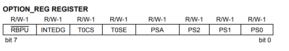
RBPU: PORTB Pull-up Enable bit (This bit is not used for timers)
1 = PORTB pull-ups are disabled
0 = PORTB pull-ups are enabled by individual port latch values
INTEDG Interrupt Edge Select bit
1 = Interrupt on the rising edge of RB0/INT pin
0 = Interrupt on the falling edge of RB0/INT pin
T0CS: TMR0 Clock Source Select bit
1 = Transition on T0CKI pin
0 = Internal instruction cycle clock (CLKO)
T0SE: TMR0 Source Edge Select bit
1 = Increment on high-to-low transition on T0CKI pin
0 = Increment on low-to-high transition on T0CKI pin
PSA: Prescaler Assignment bit
1 = Prescaler is assigned to the WDT
0 = Prescaler is assigned to the Timer0 module
PS2:PS0: Prescaler Rate Select bits

Note: There is only one Prescaler available which is mutually exclusively shared between the Timer0 module and the Watchdog Timer. A Prescaler assignment for the Timer0 module means that there is no Prescaler for the Watchdog Timer and vice versa. This Prescaler is not accessible but can be configured using PS2:PS0 bits of OPTION_REG.
PIE1 Register
The PIE1 register contains the individual enable bits for the peripheral interrupts.

PSPIE: Parallel Slave Port Read/Write Interrupt Enable bit(1)
1 = Enables the PSP to read/write interrupt
0 = Disables the PSP read/write interrupt
Note (1): PSPIE is reserved on PIC16F873A/876A devices; always maintain this bit clear.
ADIE: A/D Converter Interrupt Enable bit
1 = Enables the A/D converter interrupt
0 = Disables the A/D converter interrupt
RCIE: USART Receive Interrupt Enable bit
1 = Enables the USART to receive interrupt
0 = Disables the USART receive interrupt
TXIE: USART Transmit Interrupt Enable bit
1 = Enables the USART to transmit interrupt
0 = Disables the USART transmit interrupt
SSPIE: Synchronous Serial Port Interrupt Enable bit
1 = Enables the SSP interrupt
0 = Disables the SSP interrupt
CCP1IE: CCP1 Interrupt Enable bit
1 = Enables the CCP1 interrupt
0 = Disables the CCP1 interrupt
TMR2IE: TMR2 to PR2 Match Interrupt Enable bit
1 = Enables the TMR2 to PR2 match interrupt
0 = Disables the TMR2 to PR2 match interrupt
TMR1IE: TMR1 Overflow Interrupt Enable bit
1 = Enables the TMR1 overflow interrupt
0 = Disables the TMR1 overflow interrupt
PIR1 Register
The PIR1 register contains the individual flag bits for the peripheral interrupts.
Note: Interrupt flag bits are set when an interrupt condition occurs regardless of the state of its corresponding enable bit or the global enable bit, GIE (INTCON<7>). User software should ensure the appropriate interrupt bits are clear prior to enabling an interrupt.

PSPIF: Parallel Slave Port Read/Write Interrupt Flag bit(1)
1 = A read or a write operation has taken place (must be cleared in software)
0 = No read or write has occurred
Note (1): PSPIF is reserved on PIC16F873A/876A devices; always maintain this bit clear.
ADIF: A/D Converter Interrupt Flag bit
1 = An A/D conversion completed
0 = The A/D conversion is not complete
RCIF: USART Receive Interrupt Flag bit
1 = The USART receive buffer is full
0 = The USART receive buffer is empty
TXIF: USART Transmit Interrupt Flag bit
1 = The USART transmit buffer is empty
0 = The USART transmit buffer is full
SSPIF: Synchronous Serial Port (SSP) Interrupt Flag bit
CCP1IF: CCP1 Interrupt Flag bit
TMR2IF: TMR2 to PR2 Match Interrupt Flag bit
1 = TMR2 to PR2 match occurred (must be cleared in software)
0 = No TMR2 to PR2 match occurred
TMR1IF: TMR1 Overflow Interrupt Flag bit
1 = TMR1 register overflowed (must be cleared in software)
0 = TMR1 register did not overflow
PIE2 Register
The PIE2 register contains the individual enable bits for the CCP2 peripheral interrupt, the SSP bus collision interrupts, EEPROM writes operation interrupt, and the comparator interrupt.

CMIE: Comparator Interrupt Enable bit
1 = Enables the comparator interrupt
0 = Disable the comparator interrupt
EEIE: EEPROM Write Operation Interrupt Enable bit
1 = Enable EEPROM write interrupt
0 = Disable EEPROM write interrupt
BCLIE: Bus Collision Interrupt Enable bit
1 = Enable bus collision interrupt
0 = Disable bus collision interrupt
CCP2IE: CCP2 Interrupt Enable bit
1 = Enables the CCP2 interrupt
0 = Disables the CCP2 interrupt
PIR2 Register
The PIR2 register contains the flag bits for the CCP2 interrupt, the SSP bus collision interrupt, the EEPROM write operation interrupt, and the comparator interrupt.

CMIF: Comparator Interrupt Flag bit
1 = The comparator input has changed (must be cleared in software)
0 = The comparator input has not changed
EEIF: EEPROM Write Operation Interrupt Flag bit
1 = The write operation completed (must be cleared in software)
0 = The write operation is not complete or has not been started
BCLIF: Bus Collision Interrupt Flag bit
1 = A bus collision has occurred in the SSP when configured for I2C Master mode
0 = No bus collision has occurred
CCP2IF: CCP2 Interrupt Flag bit
Serial Interrupt – PIC16F877A Interrupt Tutorial
Circuit Diagram:
LCD:
RS – RC0
RW – RC1
EN – RC2
Data Lines – Port D
UART:
TX – RC6
RX – RC7

Programming:
In this program, I have added only the main code. You can find the header files and full project here. My PCLK is 11.0592MHz.
#include<pic.h>
#include"serial.h"
#include"lcd.h"

__CONFIG( FOSC_HS & WDTE_OFF & PWRTE_OFF & CP_OFF & BOREN_ON & LVP_OFF & CPD_OFF & WRT_OFF & DEBUG_OFF);

#define delay for(z=0;z<=50000;z++)

unsigned int z;

void interrupt ser();

void main()
{
TRISD=0;
    INTCON|=0b11000000;
    PIE1=0b00100000;
    lcd_init();
    serial_init();
    while(1) {
        cmd(0x01);
    }
}

void interrupt ser()
{
    unsigned char a = RCREG;
    tx(a);
    cmd(0x80);
    show("Serial interrupt");
    cmd(0xc0);
    show("  Key : ");
    cmd(0xc8);
    dat(a);
    delay;delay;
}
Output:
Here I pressed ‘O’ in UART Terminal. Then it is displayed in the LCD Module.

Timer Interrupt – PIC16F877A Interrupt Tutorial
Circuit Diagram:
LCD:
RS – RC0
RW – RC1
EN – RC2
Data Lines – Port D
Programming:
In this program, I have added only the main code. You can find the header files and full project here. My PCLK is 11.0592MHz.
#include<pic.h>
#include"lcd.h"

#define delay for(z=0;z<=50000;z++)

unsigned int z;

int a=0,b=0,c=0;

void interrupt tmr0()
{
    if(TMR0IF) {
        a++;
        if(a==42)                   //1sec
        {
            cmd(0x80);
            show("Timer 0 interupt");
            a=0;
            delay;
        }
        TMR0IF=0;
    } else if(TMR1IF) {
        b++;
        if(b==84)                   //2secs
        {
            cmd(0xc0);
            show("Timer 1 interupt");
            b=0;
            delay;
        }
        TMR1IF=0;
    } else if(TMR2IF) {
        c++;
        if(c==2025)                 //3secs
        {
            cmd(0x80);
            show("Timer 2 interupt");
            c=0;
            delay;
        }
        TMR2IF=0;
    }

}

void intr_init()
{
    INTCON=0xe0;
    PIE1=0x03;
}

void timer_init()
{
    OPTION_REG=0b00000111;      //internal clk,rising edge,prescaler with tim0,256
    T1CON=0b00000001;           //prescale=1,oscilator is off,internal clk,timer on
    T2CON=0b01111100;           //postscale=16,prescale=1,timer on
}

void main()
{
    lcd_init();
    timer_init();
    intr_init();
    while(1) {
        cmd(0x01);
    }
}
Output:
In this tutorial timer 0 generates an interrupt on 1sec. Timer 1 generates interrupts in 2 secs. Timer 2 generates 3secs. Each interrupts will display the interrupt in the LCD Module.
 [ Please find the output image Here ]
External Interrupt – PIC16F877A Interrupt Tutorial
Circuit Diagram:
LED – RD0
Switch – RB0

Programming:
You can find the header files and full project here. My PCLK is 11.0592MHz.
#include<pic.h>

#define LED PORTD

void interrupt  ISR(void)
{
    unsigned int i,j;
    LED=0X55;
    for(i=0;i<600;i++)
    for(j=0;j<200;j++);
    INTF=0;
}


void main(void)
{
    LED=0;
    TRISB0=1;
    TRISD=0;
    OPTION_REG=0X00;        //falling edge int @ enable pullup portb
    INTCON|=0Xd0;
    while(1) {
        LED=0x00;
    }
}
Output:
Whenever I press the switch it generates the interrupt and glows the LED. The switch is connected to an External interrupt pin.
 [ Please find the output image Here ]
In our next tutorial, we will see how to use the multiple external interrupts in PIC16F877A.
You can also read the below tutorials.
Embedded Software | Firmware | Linux Devic Driver | RTOS
Hi, I am a tech blogger and an Embedded Engineer. I am always eager to learn and explore tech-related concepts. And also, I wanted to share my knowledge with everyone in a more straightforward way with easy practical examples. I strongly believe that learning by doing is more powerful than just learning by reading. I love to do experiments. If you want to help or support me on my journey, consider sharing my articles, or Buy me a Coffee! Thank you for reading my blog! Happy learning!
Share this:

Discover more from EmbeTronicX
Subscribe to get the latest posts sent to your email.
Doesn’t anyone use MPASM anymore. I can’t find any interrupt examples using MPASM code.
Dan Laskowski
Nice information, but one question, about this line of yours
TXIF=RCIF=0; .. in the 1st example… I think that the pic16f877a wont let you write this register, its only read only.. and it will be set to 0 as soon it finished to read all the remaining characters in the buffer. isnt this correct?
Hi Alexander Zuñiga,
Thank you. Ya you are correct. Those bits are Read Only bits, software cant change that. We’ve updated that.