
This article is a continuation of the series of tutorials on the PIC16F877A Microcontroller. The aim of this series is to provide easy and practical examples that anyone can understand. In our previous tutorial, we have seen PIC16F877A USART Tutorial. Now we are going to see the PIC16F877A – Analog-to-digital Tutorial.
This article serves as a practical guide for those looking to work with the ADC module of the PIC16F877A microcontroller, providing explanations, code, and a circuit diagram to help users understand and implement this functionality in their projects.
Table of Contents
PIC16F877A ADC Tutorial
Prerequisites
Introduction
Microcontrollers are very useful especially when communicating with other devices, such as sensors, motors, switches, memory, and even other microcontrollers.
As we all know, many interface methods have been developed over the years to solve the complex problems of balancing the needs of features, cost, size, power consumption, reliability, etc.
But the ADC Analog-to-Digital converter remains famous among all. Using this ADC, we can connect any type of Analog sensor.
|
|
|
PIC16F877A ADC Module
The Analog-to-Digital (A/D) Converter module has eight of the 40/44-pin devices.
The conversion of an analog input signal results in a corresponding 10-bit digital number. The A/D module has a high and low-voltage reference input that is software selectable to some combination of VDD, VSS, RA2, or RA3.
The A/D converter has the unique feature of being able to operate while the device is in Sleep mode. To operate in Sleep, the A/D clock must be derived from the A/D’s internal RC oscillator.
PIC16F877A ADC Pins
| ADC Channel | Pin |
|---|---|
| Channel 0 | RA0/AN0 (Port A) |
| Channel 1 | RA1/AN1 (Port A) |
| Channel 2 | RA2/AN2/VRef- (Port A) |
| Channel 3 | RA3/AN3/VRef+ (Port A) |
| Channel 4 | RA5/AN4 (Port A) |
| Channel 5 | RE0/AN5 (Port E) |
| Channel 6 | RE1/AN6 (Port E) |
| Channel 7 | RE2/AN7 (Port E) |
Registers used for ADC
- A/D Control Register 0 (ADCON0)
- A/D Control Register 1 (ADCON1)
- A/D Result High Register (ADRESH)
- A/D Result Low Register (ADRESL)
A/D Control Register 0 (ADCON0)
The ADCON0 register, shown in the below image, controls the operation of the A/D module i.e. Used to Turn ON the ADC, Select the Sampling Freq, and Start the conversion.
|
|
|
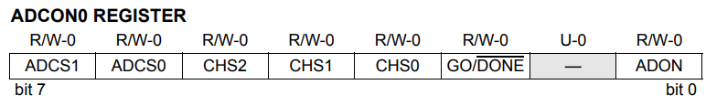
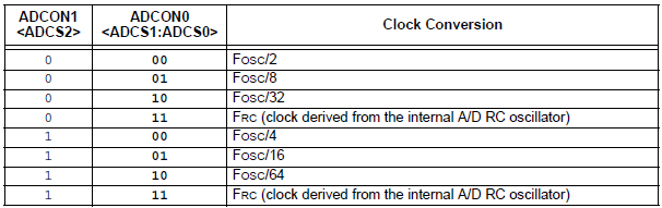
ADCS1-ADCS0: A/D Conversion Clock Select bits. These bits are based on ADCON1 Reister’s ADCS2 bit.
CHS2-CHS0: Analog Channel Select bits
000 = Channel 0 (AN0)
001 = Channel 1 (AN1)
010 = Channel 2 (AN2)
011 = Channel 3 (AN3)
100 = Channel 4 (AN4)
101 = Channel 5 (AN5)
110 = Channel 6 (AN6)
111 = Channel 7 (AN7)
|
|
|
GO/DONE: A/D Conversion Status bit
When ADON = 1:
1 = A/D conversion in progress (setting this bit starts the A/D conversion, which is automatically cleared by hardware when the A/D conversion is complete)
0 = A/D conversion not in progress
ADON: A/D On bit
1 = A/D converter module is powered up
0 = A/D converter module is shut off and consumes no operating current
A/D Control Register 1 (ADCON1)
The ADCON1 register, shown below, configures the functions of the port pins, i.e. used to configure the GPIO pins for ADC. The port pins can be configured as analog inputs (RA3 can also be the voltage reference) or as digital I/O.
|
|
|
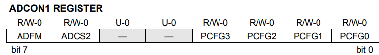
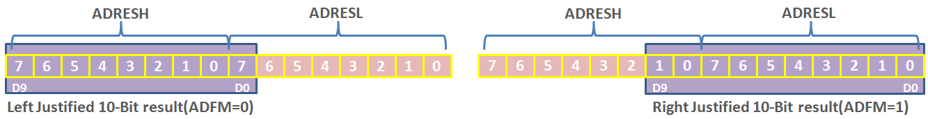
ADFM: A/D Result Format Select bit
1 = Right justified. Six (6) Most Significant bits of ADRESH are read as ‘0’.
0 = Left justified. Six (6) Least Significant bits of ADRESL are read as ‘0’.
 ADCS2: A/D Conversion Clock Select bit
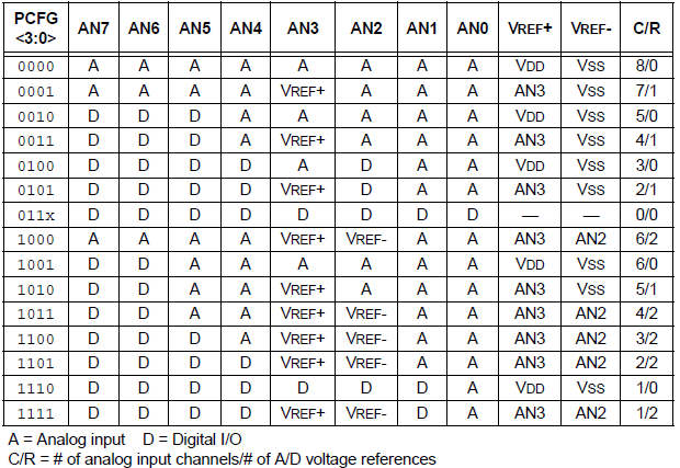
PCFG3-PCFG0: A/D Port Configuration Control bits
|
|
|
A/D Result High Register (ADRESH) & A/D Result Low Register (ADRESL)
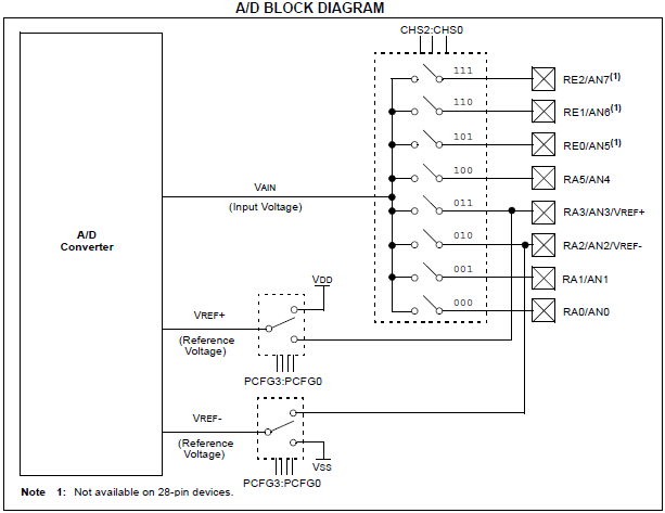
The ADRESH: ADRESL registers contain the 10-bit result of the A/D conversion. When the A/D conversion is complete, the result is loaded into this A/D Result register pair, the GO/DONE bit (ADCON0<2>) is cleared and the A/D interrupt flag bit ADIF is set. The block diagram of the A/D module is shown below.
Steps to follow
To do an A/D Conversion, follow these steps:
1. Configure the A/D module:
• Configure analog pins/voltage reference and digital I/O (ADCON1)
• Select A/D input channel (ADCON0)
• Select A/D conversion clock (ADCON0)
• Turn on A/D module (ADCON0)
|
|
|
2. Configure A/D interrupt (if desired):
• Clear ADIF bit
• Set ADIE bit
• Set PEIE bit
• Set GIE bit
3. Wait the required acquisition time.
4. Start conversion:
• Set GO/DONE bit (ADCON0)
|
|
|
5. Wait for A/D conversion to complete by either:
• Polling for the GO/DONE bit to be cleared (interrupts disabled); OR
• Waiting for the A/D interrupt
6. Read A/D Result register pair (ADRESH: ADRESL), clear bit ADIF if required.
7. For the next conversion, go to step 1 or step 2 as required.
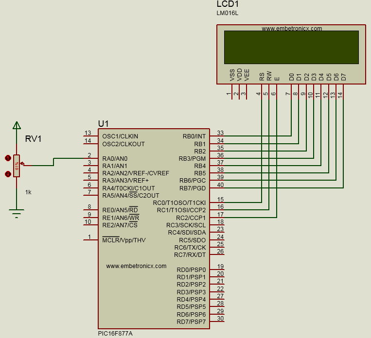
Circuit Diagram
LCD:
|
|
|
RS – RC0
RW – RC1
EN – RC2
Data Lines – Port B
POT:
|
|
|
Out – RA0
Programming
Whenever the value changes in the Potentiometer it will display in the LCD Module. In this pin, you can connect any sensors. You can download the full project here.
#include<pic.h>
#define delay for(i=0;i<=1000;i++)
#define rs RC0
#define rw RC1
#define e RC2

__CONFIG( FOSC_HS & WDTE_OFF & PWRTE_OFF & CP_OFF & BOREN_ON & LVP_OFF & CPD_OFF & WRT_OFF & DEBUG_OFF);

void adc();

void lcd_int();
void cmd(unsigned char a);
void dat(unsigned char b);
void show(unsigned char *s);

int i;

void main()
{
    TRISB=TRISC=0;          //Port B and Port C is Output (LCD)
    TRISA0=1;               //RA0 is input (ADC)
    lcd_int();
    show("ADC Value :");
    while(1) {
        cmd(0x8C);
        adc();
    }
}

void lcd_int()
{
    cmd(0x38);
    cmd(0x0c);
    cmd(0x06);
    cmd(0x80);
}

void cmd(unsigned char a)
{
    PORTB=a;
    rs=0;
    rw=0;
    e=1;
    delay;
    e=0;
}

void dat(unsigned char b)
{
    PORTB=b;
    rs=1;
    rw=0;
    e=1;
    delay;
    e=0;
}

void show(unsigned char *s)
{
    while(*s) {
        dat(*s++);
    }
}

void adc()
{
    unsigned int adcval;

    ADCON1=0xc0;                    //right justified
    ADCON0=0x85;                    //adc on, fosc/64
    while(GO_nDONE);                //wait until conversion is finished
    adcval=((ADRESH<<8)|(ADRESL));    //store the result
    adcval=(adcval/3)-1;
    dat((adcval/1000)+48);
    dat(((adcval/100)%10)+48);
    dat(((adcval/10)%10)+48);
    dat((adcval%10)+48);
}
Output – PIC16F877A ADC Tutorial
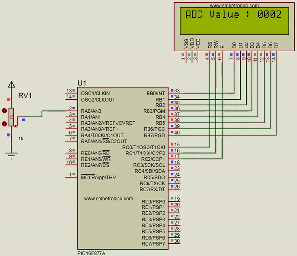 [ Please find the output image Here ]
In our next tutorial, we will see how to use the I2C in PIC16F877A.
|
|
|
You can also read the below tutorials.
Embedded Software | Firmware | Linux Devic Deriver | RTOS
Hi, I am a tech blogger and an Embedded Engineer. I am always eager to learn and explore tech-related concepts. And also, I wanted to share my knowledge with everyone in a more straightforward way with easy practical examples. I strongly believe that learning by doing is more powerful than just learning by reading. I love to do experiments. If you want to help or support me on my journey, consider sharing my articles, or Buy me a Coffee! Thank you for reading my blog! Happy learning!
