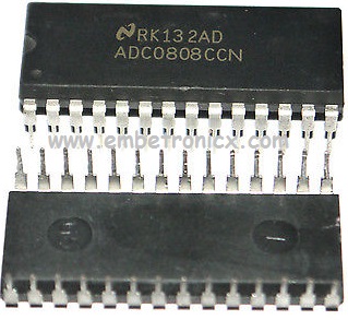
We had already seen ADC0804 Interfacing in our previous tutorial. So this Tutorial is all about ADC0808 Interfacing with 8051.
Table of Contents
Suggestion to read
Introduction
In embedded systems microcontrollers needs to take analog input. Most of the sensors & transducers such as temperature, humidity, pressure, are analog. For interfacing these sensors to microcontrollers we require to convert the analog output of these sensors to digital so that the controller can read it. Some microcontrollers have built-in Analog to Digital Convertor (ADC) so there is no need for external ADC. For microcontrollers that don’t have internal ADC external ADC is used.
Why we are using ADC for 8051 Microcontroller?
Well. 8051 doesn’t have an inbuilt ADC. So we have to use external ADC. There are many ADCs available.
-
ADC 0804
-
ADC 0808
ADC0808
One of the most commonly used ADC is ADC0808. ADC 0808 is a Successive approximation type with 8 channels i.e. it can directly access 8 single-ended analog signals. The difference between ADC0804 and ADC0808 is the number of analog input signals. I mean, In ADC0804 we can give only one analog input. But in ADC0808 we can give 8 analog inputs. So if you want to interface more analog sensors, please select ADC0808.
ADC0808 is an 8 bit analog to digital converter with eight input analog channels, i.e., it can take eight different analog inputs. The input which is to be converted to digital form can be selected by using three address lines. The voltage reference can be set using the Vref+ and Vref- pins. The step size is decided based on the set reference value. Step size is the change in analog input to cause a unit change in the output of ADC. The default step size is 19.53mV corresponding to 5V reference voltage. ADC0808 needs an external clock to operate, unlike ADC0804 which has an internal clock. The ADC needs some specific control signals for its operations like start conversion and brings data to output pins. When the conversion is complete the EOC pins go low to indicate the end of conversion and data ready to be picked up.
Features
- Easy interface to all microprocessors
- Operates ratio metrically or with 5 V DC or analog span adjusted voltage reference
- No zero or full-scale adjust required
- 8-channel multiplexer with address logic
- 0V to 5V input range with single 5V power supply
- Outputs meet TTL voltage level specifications
- Standard hermetic or molded 28-pin DIP package
- 28-pin molded chip carrier package
Pin Diagram
Pin Description
| Pin No | Function | Name |
|---|---|---|
| 1 | Analog Input Pin 3 | IN3 |
| 2 | Analog Input Pin 4 | IN4 |
| 3 | Analog Input Pin 5 | IN5 |
| 4 | Analog Input Pin 6 | IN6 |
| 5 | Analog Input Pin 7 | IN7 |
| 6 | Start conversion; input pin; a low to high pulse is given | START |
| 7 | End of conversion; output pin; goes low when the conversion is over | EOC |
| 8 | Digital output bit | D3 |
| 9 | Input pin; a low to high pulse brings data to output pins from the internal registers at end of conversion | Output Enable |
| 10 | Clock input; to provide external clock | Clock Input |
| 11 | Supply voltage; 5V | Vcc |
| 12 | Positive reference voltage | Vref+ |
| 13 | Ground (0v) | GND |
| 14 | Digital output bit | D1 |
| 15 | Digital output bit | D2 |
| 16 | Negative reference voltage | Vref- |
| 17 | Digital output bit | D0 |
| 18 | Digital output bit | D4 |
| 19 | Digital output bit | D5 |
| 20 | Digital output bit | D6 |
| 21 | Digital output bit | D7 |
| 22 | Address latch enable; Input pin; low to high pulse is required to latch in the address | ALE |
| 23 | Address line C | Address C |
| 24 | Address line B | Address B |
| 25 | Address line A | Address A |
| 26 | Analog Input Pin 0 | IN0 |
| 27 | Analog Input Pin 1 | IN1 |
| 28 | Analog Input Pin 2 | IN2 |
Selection of Channel
We can select any input channel by using the Address lines ADD A, ADD B and ADD C). We can select the input line IN0 by keeping all three address lines (ADD A, ADD B, and ADD C) Low. If we want to select input channel IN4 then we need to keep ADD A, ADD B low and ADD C high. For selecting all the other input channels, have a look on the given table:
|
|
|
| ADC Channel Name | ADD C | ADD B | ADD A |
|---|---|---|---|
| IN0 | LOW | LOW | LOW |
| IN1 | LOW | LOW | HIGH |
| IN2 | LOW | HIGH | LOW |
| IN3 | LOW | HIGH | HIGH |
| IN4 | HIGH | LOW | LOW |
| IN5 | HIGH | LOW | HIGH |
| IN6 | HIGH | HIGH | LOW |
| IN7 | HIGH | HIGH | HIGH |
Calculating Step Size
ADC 0808 is an 8 bit ADC i.e. it divides the voltage applied at Vref+ & Vref- into 28 i.e. 256 steps.
Step Size = (Vref+ - Vref-)/256
Suppose Vref+ is connected to Vcc i.e. 5V & Vref- is connected to the Gnd then the step size will be
Step size= (5 - 0)/256= 19.53 mv
|
|
|
How to use the ADC0808?
- Start
- Select the channel.
- A Low – High transition on ALE to latch in the address.
- A Low – High transition on Start to reset the ADC’s SAR.
- A High – Low transition on ALE.
- A High – Low transition on start to start the conversion.
- Wait for the End of cycle (EOC) pin to become high.
- Make Output Enable pin High.
- Take Data from the ADC’s output
- Make Output Enable pin Low.
- Stop
ADC0808 interfacing with 8051
Circuit Diagram
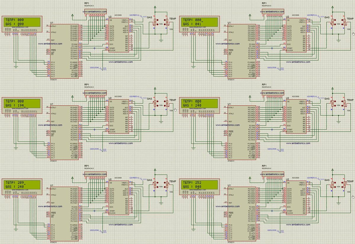
In this tutorial, I’m going to connect the PotentioMeter (Variable Resistor) instead of the real sensor. You can connect the real sensor to Hardware.
LCD:
- RS – P1.0
- RW – GND
- EN – P1.1
- LCD Data Lines – P1 LSB 4 bits
ADC:
- Output Enable – P2.0
- EOC – P2.1
- Start – P2.2
- Addr A – P2.4
- Addr B – P2.5
- Addr C – P2.6
- ALE – P2.7
- ADC Data lines – Po
Code
You can download the entire project here.
|
|
|
#include<reg51.h>

#define adc_data P0
#define lcd    P1

unsigned char temp, gas;

sbit rs=P1^0;
sbit en=P1^1;

sbit OE     =P2^0;
sbit EOC    =P2^1;
sbit START  =P2^2;
sbit AA     =P2^4;
sbit BB     =P2^5;
sbit CC     =P2^6;
sbit ALE    =P2^7;

unsigned char adc_val;

void lcd_init();
void cmd(unsigned char a);
void dat(unsigned char b);
void show(unsigned char *s);
void lcd_delay();

unsigned char adc(unsigned int ch);
void ch_sel(unsigned int sel);

void  main()
{
    lcd_init();
    show("TEMP: ");
    cmd(0xc0);
    show("GAS : ");
    while(1) {
        cmd(0x86);
        temp=adc(0);                 //Reading Value from ADC Channel 0
        dat((temp/100)%10 +0x30);
        dat((temp/10)%10 +0x30);
        dat(temp%10 +0x30);

        cmd(0xc6);
        gas=adc(1);                 //Reading Value from ADC Channel 1
        dat((gas/100)%10 +0x30);
        dat((gas/10)%10 +0x30);
        dat(gas%10 +0x30);
    }
}

void lcd_init()
{
    cmd(0x02);
    cmd(0x28);
    cmd(0x0e);
    cmd(0x06);
    cmd(0x80);
}

void cmd(unsigned char a)
{
    rs=0;
    lcd&=0x0F;
    P1|=(a&0xf0);
    en=1;
    lcd_delay();
    en=0;
    lcd_delay();
    lcd&=0x0f;
    lcd|=(a<<4&0xf0);
    en=1;
    lcd_delay();
    en=0;
    lcd_delay();
}

void dat(unsigned char b)
{
    rs=1;
    lcd&=0x0F;
    lcd|=(b&0xf0);
    en=1;
    lcd_delay();
    en=0;
    lcd_delay();
    lcd&=0x0f;
    lcd|=(b<<4&0xf0);
    en=1;
    lcd_delay();
    en=0;
    lcd_delay();
}

void show(unsigned char *s)
{
    while(*s) {
        dat(*s++);
    }
}

void lcd_delay()
{
    unsigned int lcd_delay;
    for(lcd_delay=0;lcd_delay<=1000;lcd_delay++);
}

unsigned char adc(unsigned int ch)
{
    adc_data=0xff;

    ALE=START=OE=AA=BB=CC=0;
    EOC=1;

    ch_sel(ch);

    ALE=1;
    START=1;
    ALE=0;
    START=0;
    while(EOC==1);
    while(EOC==0);
    OE=1;
    adc_val=adc_data;
    OE=0;
    return adc_val;
}

void ch_sel(unsigned int sel)
{
    switch(sel) {
        case 0: CC=0;BB=0;AA=0; break;          //000
        case 1: CC=0;BB=0;AA=1; break;          //001
        case 2: CC=0;BB=1;AA=0; break;          //010
        case 3: CC=0;BB=1;AA=1; break;          //011
        case 4: CC=1;BB=0;AA=0; break;          //100
        case 5: CC=1;BB=0;AA=1; break;          //101
        case 6: CC=1;BB=1;AA=0; break;          //110
        case 7: CC=1;BB=1;AA=1; break;          //111
    }
}
Output – ADC0808 interfacing with 8051
 [ Please find the output image Here ]
In our next tutorial, we will see an Ultrasonic sensor interfacing with the 8051.
You can also read the below tutorials.
|
|
|

Embedded Software | Firmware | Linux Devic Deriver | RTOS
Hi, I am a tech blogger and an Embedded Engineer. I am always eager to learn and explore tech-related concepts. And also, I wanted to share my knowledge with everyone in a more straightforward way with easy practical examples. I strongly believe that learning by doing is more powerful than just learning by reading. I love to do experiments. If you want to help or support me on my journey, consider sharing my articles, or Buy me a Coffee! Thank you for reading my blog! Happy learning!


