This article is a continuation of the Series on STM32 Bootloader and carries the discussion on Bootloader design and implementation. The aim of this series is to provide easy and practical examples that anyone can understand.
This post is about the Bootloader in STM32F76xxx (Bootloader Design) where we discuss how to design a bootloader.
We have attached the video explanation at the bottom of this post.
Table of Contents
Prerequisites
In this tutorial, we will be using the concepts that have been explained already in the tutorial. So I would request you to go through those tutorials first if you are not familiar with those topics.
Introduction
In our last post, we discussed what is a bootloader and why we need that in our project. From this post, we will jump into bootloader implementation.
|
|
|
Before implementing the bootloader, we must know how our bootloader should be. So, we have to design our custom bootloader. We will design our own custom bootloader.
Hardware Required
- STM32F767Zi Nucleo (You can use any STM32 boards. But use the addresses based on your controller).
- LED (If you don’t have onboard LED)
Bootloader in STM32F76xxx
Before designing the bootloader, If you know what happens when you press the reset button in the microcontroller, that will be helpful for you to understand better.
Features of STM32F767Zi
- Core: Arm® 32-bit Cortex®-M7 CPU with DPFPU, ART Accelerator, and L1-cache: 16 Kbytes I/D cache, allowing 0-wait state execution from embedded Flash and external memories, up to 216 MHz, MPU, 462 DMIPS/2.14 DMIPS/MHz (Dhrystone 2.1), and DSP instructions.
- Dual-mode Quad-SPI
- Graphics
- Chrom-ART Accelerator (DMA2D), a graphical hardware accelerator enabling enhanced graphical user interface
- Hardware JPEG codec
- LCD-TFT controller supporting up to XGA resolution
- MIPI® DSI host controller supporting up to 720p 30 Hz resolution
- Clock, reset, and supply management
- 1.7 V to 3.6 V application supply and I/Os
- POR, PDR, PVD, and BOR
- Dedicated USB power
- 4-to-26 MHz crystal oscillator
- Internal 16 MHz factory-trimmed RC (1% accuracy)
- 32 kHz oscillator for RTC with calibration
- Internal 32 kHz RC with calibration
- Low-power
- Sleep, Stop, and Standby modes
- VBAT supply for RTC, 32×32 bit backup registers + 4 Kbytes backup SRAM
- 3×12-bit, 2.4 MSPS ADC: up to 24 channels
- Digital filters for sigma-delta modulator (DFSDM), 8 channels / 4 filters
- 2×12-bit D/A converters
- General-purpose DMA: 16-stream DMA controller with FIFOs and burst support
- Up to 18 timers: up to thirteen 16-bit (1x low-power 16-bit timer available in Stop mode) and two 32-bit timers, each with up to 4 IC/OC/PWM or pulse counter and quadrature (incremental) encoder input. All 15 timers run up to 216 MHz. 2x watchdogs, SysTick timer
- Debug mode
- SWD and JTAG interfaces
- Cortex®-M7 Trace Macrocell™
- Up to 168 I/O ports with interrupt capability
- Up to 164 fast I/Os up to 108 MHz
- Up to 166 5 V-tolerant I/Os
- Up to 28 communication interfaces
- Up to 4 I2C interfaces (SMBus/PMBus)
- Up to 4 USARTs/4 UARTs (12.5 Mbit/s, ISO7816 interface, LIN, IrDA, modem control)
- Up to 6 SPIs (up to 54 Mbit/s), 3 with muxed simplex I2S for audio
- 2 x SAIs (serial audio interface)
- 3 × CANs (2.0B Active) and 2x SDMMCs
- SPDIFRX interface
- HDMI-CEC
- MDIO slave interface
- Advanced connectivity
- USB 2.0 full-speed device/host/OTG controller with on-chip PHY
- USB 2.0 high-speed/full-speed device/host/OTG controller with dedicated DMA, on-chip full-speed PHY, and ULPI
- 10/100 Ethernet MAC with dedicated DMA: supports IEEE 1588v2 hardware, MII/RMII
- 8- to the 14-bit camera interface up to 54 Mbyte/s
- True random number generator
- CRC calculation unit
- RTC: subsecond accuracy, hardware calendar
- 96-bit unique ID
Memory in STM32F767Zi
- Up to 2 Mbytes of Flash memory organized into two banks allowing read-while-write
- SRAM: 512 Kbytes (including 128 Kbytes of data TCM RAM for critical real-time data) + 16 Kbytes of instruction TCM RAM (for critical real-time routines) + 4 Kbytes of backup SRAM
- Flexible external memory controller with up to 32-bit data bus: SRAM, PSRAM, SDRAM/LPSDR SDRAM, NOR/NAND memories
Flash Memory in STM32F767Zi
- Flash memory read operations with two data width modes supported:
- Single bank mode nDBANK=1: read access of 256 bits
- Dual bank mode nDBANK=0: read access of 128 bits
- Flash memory program/erase operations
- Read/write protections
- Read While Write (RWW) (only possible in dual bank mode nDBANK=0)
- Dual Boot mode (only possible in dual bank mode nDBANK=0)
- ART Accelerator™: 64 cache lines of 128/256 bits on the ITCM interface (depending on read access width)
- Prefetch on TCM instruction code
In this tutorial series, we will be using flash memory as a single bank mode. The single blank is divided into multiple sectors as given below.

Boot modes
We will discuss the boot modes that are available in the STM32F767xxx devices. When you press the reset button, the processor starts running from the 0x00000000 address.
|
|
|
But we can change this by using these boot modes. Every microcontroller has one or a few boot pins. Using that we can tell the processor to start from the address that we want.
To know the boot modes of your STM32 devices, please go through your STM32’s reference manual. STM32F76xxx has only one boot pin (not two). Refer to the below image which has been taken from the datasheet.

Here If the BOOT0 pin is grounded, then it will start from the address 0x00200000. If the BOOT0 pin is high during the power-up, it will start from the address 0x00100000 where the System bootloader sits.
But we don’t want to run the system bootloader. We want to run our bootloader. In that case, we can keep the BOOT0 pin grounded and place our bootloader code into 0x08000000.
|
|
|
I know you will get confused. We are placing our bootloader code into 0x08000000 and the controller starts from 0x00200000. How that will take our bootloader?
Actually, both are pointing to the same memory. Only the difference is the bus that is used to access that memory. In STM32F767Zi, 0x00200000 will be accessed by using the ITCM bus where we have permission only to read and execute and not write.
But the address 0x08000000 will be accessed by the AXI bus where we have read, write, and execute permission. That’s why we are writing our Bootloader to that memory and the processor will read that memory using the ITCM bus. For understanding, you can assume that 0x00200000 is the alias of 0x08000000.
If you want to verify this, then write the bootloader into 0x08000000 and read the 0x00200000. The same data will be present in both addresses.
We said earlier that the microcontroller will start from the 0x00000000 address, how it is possible to change the address to some other?
|
|
|
That’s where the memory aliasing comes into the picture. If the BOOT0 pin is grounded, then 0x00200000 will act as 0x00000000. Otherwise, 0x00100000 will act as the 0x00000000. I hope you are clear now.
Note: This is valid for STM32F767Zi. Please verify your controller’s datasheet.
For more details, you can refer to the STM32F76xxx datasheet.
What is a system bootloader?
The system bootloader in STM32 is the bootloader that has been provided by the chip manufacturers. We cannot overwrite as it has loaded into the ROM memory. We can also call this a ROM bootloader. Using this bootloader, we can update the firmware or application from the bootloader.
But we cannot do many operations like updating the application wirelessly like OTA. So, writing our own bootloader in STM32 will help us to implement whatever we like.
|
|
|
Bootloader Design
We discussed some important memory-related things earlier and understood that writing our own bootloader is good instead of using the system bootloader in our project. Let’s jump to the Bootloader.
So, we will place the bootloader into 0x08000000, and when the system powers up, it will run the bootloader. Then we have to place the application into some other memory. From the bootloader, we have to call the application.
It’s simple, right? But it is not.
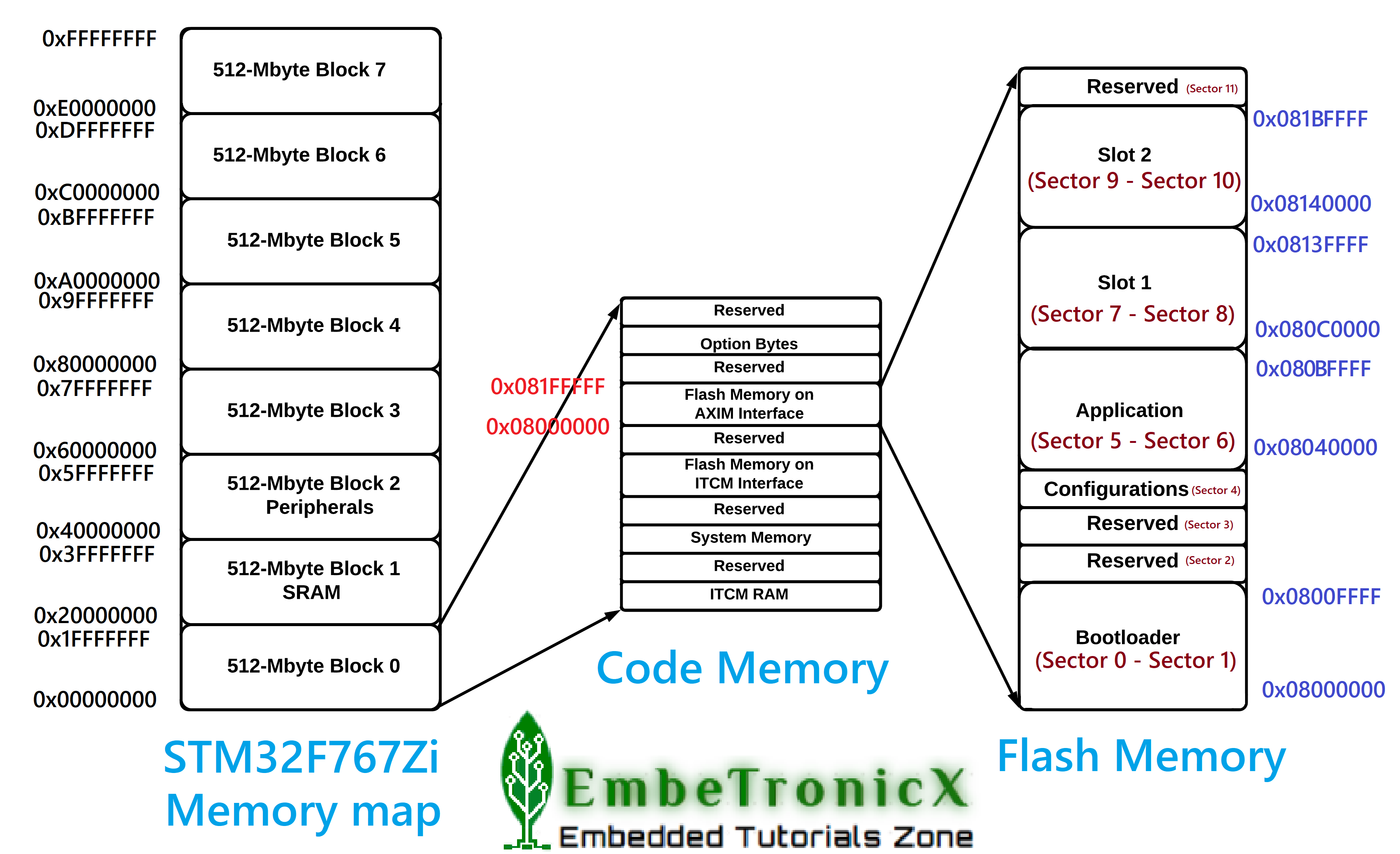
Organizing the memory
First, we have to decide, where to keep the application and bootloader. In this series, I am also going to keep the two backup spaces for the application where I store the current version of the application (Slot 1) and the previous version of the application (Slot 2).
I have a 2MB flash in STM32F767Zi. That’s why I have decided to keep two versions of the application as a backup. Based on the memory you have, you can decide the number of slots.
|
|
|
- The bootloader will be placed into the sector 0, 1 (
0x08000000to0x0800FFFF) (64KB). - The actual application will be placed into the sector 5,6 (
0x08040000to0x080BFFFF) (512KB). - Backup application will be placed into the sector 7,8 (
0x080C0000to0x0813FFFF) (512KB). - Backup application 2 will be placed into the sector 9,10 (
0x08140000to0x081BFFFF) (512KB). - Configurations will be stored in sector 3 (
0x08020000to0x0803FFFF) (128KB).
Look at the below image for a better understanding.
Now we have finalized the memory area to keep the application, bootloader, and backup applications. We have to plan the operations of the bootloader and application.
Bootloader and Application operations
I have designed the bootloader and application like the below image.

|
|
|
Note: This design is just for educational purposes. There may be something that we can improve. Some bugs also will be there in this design.
Bootloader Process Flow
Block B1
The bootloader starts when the microcontroller powers up or resets.
- Goto Block B2.
Block B2
Check the user boot button is pressed. This boot pin is not the same as the BOOT0 pin. This boot pin is our bootloader pin to identify the Firmware/Application update process.
Block B3
Receive the data from the UART.
- Goto Block B4.
Block B4
Write the received data to either slot 1 or slot 2 based on availability.
|
|
|
- Goto Block B5.
Block B5
Reset the microcontroller, So that the bootloader runs again.
Block B6
The reboot causes will be stored in a particular area. Read that reboot cause and go to Block B7, Block B8, Block B10, and Block B13.
Block B7
- If the application requests for the OTA update then go to Block B3.
Block B8
- If this is the very first time boot, then go to Block B9.
Block B9
As this is the very first boot, the bootloader will copy the application from slot 1 to the actual application area which is 0x08040000. Then go to Block B11.
Block B10
- If this is the normal boot, then go to Block B11.
Block B11
Verify the CRC from the actual application location. This will help us to identify whether the application has been modified by some hacker or any memory corruption.
- If CRC verification is successful then go to Block B12.
- If CRC verification is failed then go to Block B15.
Block B12
Give control to the application.
|
|
|
Block B13
If the application requests to load the previous application, then go to Block B14.
Block B14
Copy the old application from slot 1 or slot 2 to the actual application and go to Block B11.
Block B15
If the CRC verification is failed, then don’t run the application and stay there.
Application Process Flow
The Application process flow steps description is the following.
Block A1
The bootloader starts the application. Then go to Block A2.
|
|
|
Block A2
Check for the GPIO interrupt.
Block A3
Blink the LED.
Block A4
We have received the interrupt, Which means some OTA package is available. So, write the reboot reason as an OTA request. Then go to Block A5.
Block A5
Reset the device. So that the Bootloader will receive the OTA package and update it.
Tutorials breakdown
Our target is to implement the logic that we have explained above. We are dividing the implementation into multiple posts.
|
|
|
- Write a simple bootloader that runs the application.
- Implement the firmware/application update feature to the bootloader.
- Add some features to the bootloader like CRC check, Slot1, Slot 2, etc.
- Add the feature of updating the firmware/application wirelessly like Bluetooth or wifi to the bootloader and application.
- Firmware update using the SD Card (SPI communication)
Video Explanation
Please check our below video explanation.
In our next post, we will write the basic bootloader in STM32 that gives control to the application.
You can also read the below tutorials.
|
|
|
Embedded Software | Firmware | Linux Devic Deriver | RTOS
Hi, I am a tech blogger and an Embedded Engineer. I am always eager to learn and explore tech-related concepts. And also, I wanted to share my knowledge with everyone in a more straightforward way with easy practical examples. I strongly believe that learning by doing is more powerful than just learning by reading. I love to do experiments. If you want to help or support me on my journey, consider sharing my articles, or Buy me a Coffee! Thank you for reading my blog! Happy learning!
