This is the Series of tutorials on the STM32 Microcontroller. The aim of this series is to provide easy and practical examples that anyone can understand. Basically, you can write GPIO codes in multiple ways (Using HAL, the GPIO driver).
Using that HAL you can finish your job in very few lines of code. But I would suggest you, learn to program using the bare-metal code (without any HAL or driver) initially. This is the STM32 GPIO Tutorial without HAL.
The tutorial series covers STM32 microcontroller programming, focusing on GPIO operations without using the Hardware Abstraction Layer (HAL) or drivers. It aims to provide practical examples for easy understanding. The tutorials cover a variety of topics related to STM32 GPIO:
This tutorial aims to help beginners understand the basics of STM32 GPIO programming without relying on higher-level abstractions, making it suitable for those who want to learn the fundamentals of microcontroller interaction.
You can also read, Getting Started with STM32 RTOS, PIC16F877A GPIO tutorial, GPIO Linux device driver, and STM32 GPIO RTOS tutorial.
|
|
|
Table of Contents
STM32 GPIO Tutorial
Before starting this STM32 GPIO Tutorial, Please go through the below tutorials.
Hardware Requirements
In this tutorial, we are going to see the timer for the below three STM32 controllers. If you have any one of the controllers or ARM cortex, you can use that. Please click the controller-specific tab and see the content properly.
We have our own EmbeTronicX Store called ChipTronicX. You can purchase the hardware from ChipTronicX.
- STM32F103CBT6 (ARM Cortex M0)
- STM32F411CE (ARM Cortex M4)
- STM32F767Zi (ARM Cortex M7)
- Button
- LEDs
STM32 GPIO Tutorial – Bare Metal
In this post, we have used three microcontrollers (STM32F1, STM32F4, STM32F7) for demonstration. You can go to the section directly based on the microcontroller that you have.
- SM32F4 GPIO Registers
- STM32F1 GPIO Registers
- STM32F7 GPIO Registers
STM32F4 and STM32F7 GPIO Registers
STM32F411CE GPIO Registers
There are a couple of registers used in GPIO. I have classified these registers into 4 types based on their operation.
|
|
|
1. Control Registers
Before looking into the control register, we will see the Clock Register (RCC_AHB1ENR) which will enable the AHB clock to the GPIO ports.
RCC_AHB1ENR
This is called as RCC AHB1 peripheral clock enable register. The register is given below.
Bit [0] – GPIOAEN: IO port A clock enable
- 0 – IO port A clock disabled
- 1 – IO port A clock enabled
Bit [1] – GPIOBEN: IO port B clock enable
- 0 – IO port B clock disabled
- 1 – IO port B clock enabled
Bit [2] – GPIOBEN: IO port C clock enable
|
|
|
- 0 – IO port C clock disabled
- 1 – IO port C clock enabled
Bit [3] – GPIOBEN: IO port D clock enable
- 0 – IO port D clock disabled
- 1 – IO port D clock enabled
Bit [4] – GPIOBEN: IO port E clock enable
- 0 – IO port E clock disabled
- 1 – IO port E clock enabled
We don’t need the rest of the bits as we are only working on GPIO.
Example:
//These are a couple of ways of enabling AHB clock for Port A
SET_BIT(RCC->AHB1ENR, RCC_AHB1ENR_GPIOAEN);
RCC->AHB1ENR |= (1UL << 0U);
The below control registers are used to configure the GPIOs.
|
|
|
- GPIO Port mode register (
GPIOx_MODER) - GPIO Port output type register (
GPIOx_OTYPER) - GPIO Port output speed register (
GPIOx_OSPEEDR) - GPIO Port Pullup/Pulldown register (
GPIOx_PUPDR)
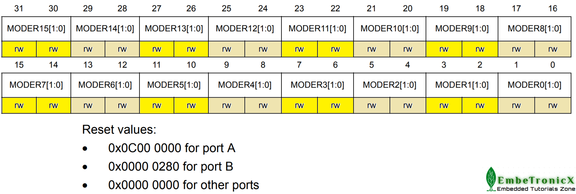
1. GPIOx_MODER:
This GPIO port mode register is used to select the I/O direction. Please find the below image of the GPIOx_MODER register.
Here 2-bits are combined for one particular GPIO pin.
Bits [31:0] – MODERy: Direction selection for port X and bit Y, (y = 0 … 15)
MODERy Direction Selection:
00: Input (reset state)
01: General purpose output mode
10: Alternate Function mode
11: Analog mode
|
|
|
In this tutorial, we are using only the I/O operation. So, we will use either Input mode or output mode.
Example:
//makes Port A0 as output
GPIOA->MODER = 0x00000001;

//makes Port A5 as output
GPIOA->MODER = 0x00000400;

//makes Port A as output
GPIOA->MODER = 0x55555555;

//makes Port A as input
GPIOA->MODER = 0x00000000;
2. GPIOx_OTYPER:
This is the GPIO output type register which is used to select the output type (Push-Pull or Open Drain). First, we need to know what is push-pull and open drain.
Open-drain output type
I think most of them are aware of this. If you have worked on I2C you must have heard this. But still, I will put my words. In open-drain mode, inside the microcontroller one switch (transistor/MOSFET) is connected to the GPIO pin and the ground.
So If you write high to the GPIO pin using software, it will be connected to the ground through the switch. Which means the original output is low.
|
|
|
If you write low to the GPIO pin, it will be left floating since the switch will be turned off. That’s why we are using a pull-up resistor for the open-drain pins.
Push-Pull output type
Whereas in push-pull mode, two switches (transistor/MOSFET) will be there inside the microcontroller. One switch is connected to Vcc/Vdd and another switch is connected to the ground. So when you write High to the GPIO pin, the switch will be connected to the Vcc/Vdd.
The resulting output will be high (1). And if you write low to the GPIO, then the switch will be connected to the ground. The resulting output will be low (0).
Do you get some idea about both output modes? Okay, let’s go to the register now. Please find the below image of the GPIOx_OTYPER register.
Here,
|
|
|
Bits [15:0] – OTy: Port output type, (y = 0 … 15)
- 0 – Output Push-Pull (reset state)
- 1 – Output open-drain
Bits [31:16] – Reserved (Must be kept at reset value).
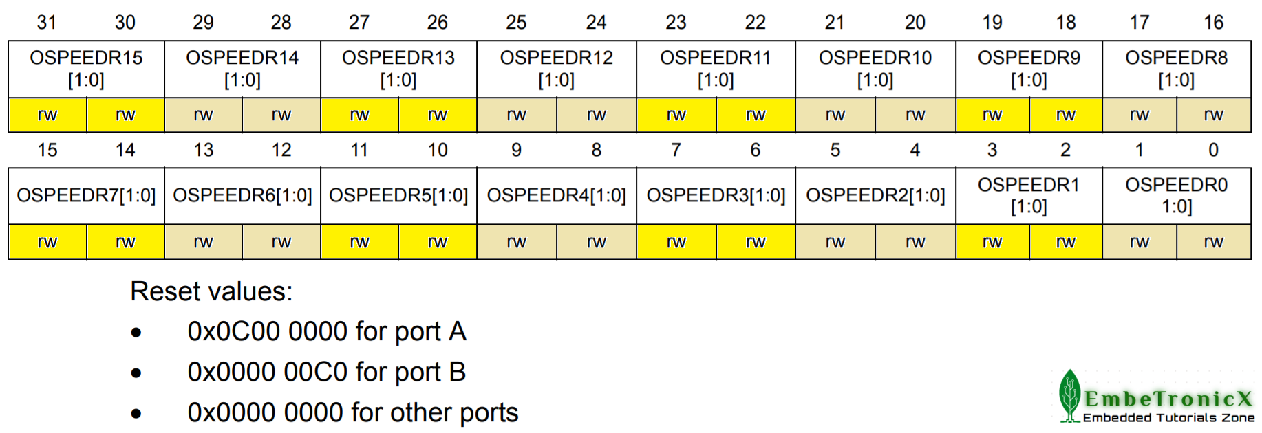
3. GPIOx_OSPEEDR:
This GPIO Output speed register is used to set the speed of the GPIO pin. Please find the below image of the GPIOx_OSPEEDR register.
Here 2-bits are combined for one particular GPIO pin.
Bits [31:0] – OSPEEDRy: Speed selection for port X and bit Y, (y = 0 … 15)
|
|
|
OSPEEDRy Selection:
00: Low Speed
01: Medium speed
10: High speed
11: Very high speed
4. GPIOx_PUPDR:
This is the GPIO port pullup/pulldown register which is used to configure the GPIO pin into Pullup or pulldown mode. Please find the below image of the GPIOx_PUPDR register.
Here 2-bits are combined for one particular GPIO pin.
Bits [31:0] – PUPDRy: pullup/pulldown selection for port X and bit Y, (y = 0 … 15)
|
|
|
PUPDRy Selection:
00: No pullup or pulldown
01: Pullup
10: Pulldown
11: Reserved
Example:
//Enable Pullup on PA0
GPIOA->PUPDR = 0x00000001;

//Enable Pullup on PA
GPIOA->PUPDR = 0x55555555;
Data Registers
These data registers are used to store the data to be output/input. The below registers are used for output/input.
- Input data register (
GPIOx_IDR) - Output data register (
GPIOx_ODR) - Bit Set/Reset register (
GPIOx_BSRR)
where, x = A, B, C, D, and E.
|
|
|
1. GPIOx_IDR:
This is the Input Data Register. When you configure the GPIO ports as input using GPIOx_MODER register, this register is used to get the value from the GPIO pin. This register is a read-only register. So you cannot write into it. Please find the below image of the GPIOx_IDR register.
Here,
Bits [15:0] – IDRy: Port Input Data, (y = 0 … 15)
This will contain the corresponding value of the corresponding I/O port. It can be accessed in 32-bit word mode only. Which means you cannot read a single bit. You have to read the whole register.
Bits [31:16] – Reserved (Must be kept at reset value).
|
|
|
Example:
Let’s assume that I have configured PORT B as input, using the GPIOB_MODER register and other control registers. Now we can read the GPIO pins like below.
//Reading PB0 bit
if( ( GPIOB->IDR & 0x01) == 0 )
{
  //PORT B's 0th bit is 0
}
else
{
  //PORT B's 0th bit is 1
}

//Reading full PB
uint32_t value = GPIOB->IDR;

//Reading PB15
bool value = (( GPIOB->IDR >> 15 ) & 0x1);
2. GPIOx_ODR:
This is the Output Data Register. When you have configured the GPIO Port as output using GPIOx_MODER register, this register is used to set the value to the GPIO pin. We can read and write to the register. Please find the below image of the GPIOx_ODR register.
Bits [15:0] – ODRy: Port Output Data, (y = 0 … 15)
We can write to the corresponding value of the corresponding I/O port.
|
|
|
Bits [31:16] – Reserved (Must be kept at reset value).
Note: When you read the output data register, it will give you the last written value.
Example:
Let’s assume that I have configured PORT B as output, using the GPIOB_MODER register and other control registers. Now we can write the GPIO pins like below.
//Write 1 to the full Port B
GPIOB->ODR = 0x0000FFFF;

//Write 0 to the full Port B
GPIOB->ODR = 0x00000000;
You have to be careful when you are writing the GPIO port using this GPIOx_ODR. Because you may disturb the other Pins (bits) of the register which you don’t want. Then what if I want to write a single bit without disturbing others? There is a way to do that. Just keep reading.
|
|
|
3. GPIOx_BSRR:
This is the GPIO Bit Set/Reset Register. When you want to set or reset a particular bit or pin, you can use this register. This is a write-only register. This register will do the atomic set/reset. So we don’t worry about the interrupts that cause problems during set/reset.
In this register, the lower 16 bits are used to set any of the 16 pins, and the higher 16 bits to clear/reset any of the 16 pins of a particular IO port. Please find the below image of the GPIOx_BSRR register.
Bits [15:0] – BSy: Port Set Bit, (y = 0 … 15)
These bits are write-only and accessed in word, half-word, or byte mode. If you read this register you will get 0x00000000. If you write 1 to any bit [0 to 15], it will set the corresponding bit in GPIOx_ODR register [0 to 15]. If you write 0 to any bit [0 to 15], no action will be performed to the corresponding bit in GPIOx_ODR register [0 to 15].
Bits [31:16] – BRy: Port Reset Bit, (y = 0 … 15)
|
|
|
These bits are write-only and accessed in word, half-word, or byte mode. If you read this register you will get 0x00000000. If you write 1 to any bit [16 to 31], it will set the corresponding bit in GPIOx_ODR register [0 to 15]. If you write 0 to any bit [0 to 15], no action will be performed to the corresponding bit in GPIOx_ODR register [0 to 15].
If you set both BSx and BRx, BSx has priority. So BRx will be ignored. Where, x = 0…15.
Example:
Let’s assume that I have configured PORT B as output, using the GPIOB_MODER register and other control registers. Now we can write the GPIO pins like below.
//set all the bits of Port B
GPIOB->BSRR = 0x0000FFFF;

//Clear all the bits of Port B
GPIOB->BSRR = 0xFFFF0000;

//Set the 5th bit of Port B
GPIOB->BSRR = (1U << 5);

//Clear the 5th bit of Port B
GPIOB->BSRR = (1U << 21);
Locking Registers
This register is used to lock the configuration of the port bits. The below register is used to do that.
|
|
|
1. GPIOx_LCKR:
Using this register, you can freeze the GPIO configurations. Once you do the proper lock key write sequence, it will lock the GPIOx_MODER, GPIOx_OTYPER, GPIOx_OSPEEDR, GPIOx_PUPDR, GPIOx_AFRL, and GPIOx_AFRH registers. Before we see how to do that, let’s see that register. Please find the below image of the GPIOx_LCKR register.
This can be accessed in 32-bit word only and you can perform both read and write.
Bits [15:0] – LCKy: Port Set Bit, (y = 0 … 15)
- 0 – Port configuration is not locked
- 1 – Port configuration is locked
These bits can be written when the LCKK (16th bit) is 0.
Bits [16] – LCKK: Lock Key
|
|
|
- 0 – Port configuration lock key is not active
- 1 – Port configuration lock key is not active
This bit can be read at any time. But if we want to modify the bit, we have to follow the Lock key write sequence. Once you have locked the GPIO, then it will be locked until an MCU reset or a peripheral reset occurs.
Bits [31:17] – Reserved (Must be kept at reset value).
Lock key write sequence
As per the datasheet, below is the lock key write sequence.
WR LCKR[16] = ‘1’ + LCKR[15:0]WR LCKR[16] = ‘0’ + LCKR[15:0]WR LCKR[16] = ‘1’ + LCKR[15:0]RD LCKRRD LCKR[16] = ‘1’ (this read operation is optional but it confirms that the lock is active)Note: During the Lock key write sequence, the value of LCK[15:0] should not change. And in some other STM32, this GPIOx_LCKR is not available for all the GPIO ports. So you should check with the datasheet before doing this. However, in the STM32F411CE, the GPIOx_LCKR register is available for all the GPIO ports.
Any error in the lock key write sequence aborts the lock. Once you have done the lock key write sequence properly on any bit of the port, any read access on the LCKK bit will return ‘1’ until the next CPU reset.
|
|
|
If you get confused, please go through the below example.
/*
** The below full code snippet, locks the GPIO configuration of Port B.5 (PB5)
*/
#define GPIO_PIN_POS (5U)    //I want to lock PB5. So setting 5th bit
#define LCKK_BIT_POS (16U)   //Position of LCKK bit

volatile uint32_t lock_gpio = 0;

/* Lock key write sequence */
/* WR LCKR[16] = ‘1’ + LCKR[5] = ‘1’ */
lock_gpio = (( 1UL << LCKK_BIT_POS) | ( 1UL << GPIO_PIN_POS ));
GPIOB->LCKR = lock_gpio;

/* WR LCKR[16] = ‘0’ + LCKR[5] should not change*/
GPIOB->LCKR = ( 1UL << GPIO_PIN_POS );

/* WR LCKR[16] = ‘1’ + LCKR[5] should not change*/
GPIOB->LCKR = lock_gpio;

/* RD LCKR */
lock_gpio = GPIOB->LCKR;
if((GPIOB->LCKR & ( 1UL << LCKK_BIT_POS)) != 0)
{
  //PB5 configuration has been locked
}
else
{
  //PB5 configuration has not been locked
}
Alternate Function Registers
Each GPIO pin has around sixteen alternative functions like SPI, I2C, UART, etc. So we can tell the STM32 to use our required functions.
The below-mentioned two registers are used to select one function out of sixteen alternative function inputs/outputs available for each I/O.
GPIOx_AFRL:
This 32-bit register is grouped by 4 bits. So This GPIOx_AFRL register is used to select the alternate functions of Pin 0 to Pin 7. Please find the below image of the GPIOx_AFRL register.
Bits [31:0] – AFRLy: Alternate function selection for port X and bit Y, (y = 0 … 7)
|
|
|
AFRLy Selection:
0000: AF0 (Alternate Function 0)
0001: AF1 (Alternate Function 1)
0010: AF2 (Alternate Function 2)
0011: AF3 (Alternate Function 3)
0100: AF4 (Alternate Function 4)
0101: AF5 (Alternate Function 5)
0110: AF6 (Alternate Function 6)
0111: AF7 (Alternate Function 7)
1000: AF8 (Alternate Function 8)
1001: AF9 (Alternate Function 9)
1010: AF10 (Alternate Function 10)
1011: AF11 (Alternate Function 11)
1100: AF12 (Alternate Function 12)
1101: AF13 (Alternate Function 13)
1110: AF14 (Alternate Function 14)
1111: AF15 (Alternate Function 15)
GPIOx_AFRH:
This 32-bit register is grouped by 4 bits. So This GPIOx_AFRH register is used to select the alternate functions of Pin 8 to Pin 15. Please find the below image of the GPIOx_AFRH register.
Bits [31:0] – AFRHy: Alternate function selection for port X and bit Y, (y = 0 … 7)
AFRHy Selection:
|
|
|
0000: AF0 (Alternate Function 0)
0001: AF1 (Alternate Function 1)
0010: AF2 (Alternate Function 2)
0011: AF3 (Alternate Function 3)
0100: AF4 (Alternate Function 4)
0101: AF5 (Alternate Function 5)
0110: AF6 (Alternate Function 6)
0111: AF7 (Alternate Function 7)
1000: AF8 (Alternate Function 8)
1001: AF9 (Alternate Function 9)
1010: AF10 (Alternate Function 10)
1011: AF11 (Alternate Function 11)
1100: AF12 (Alternate Function 12)
1101: AF13 (Alternate Function 13)
1110: AF14 (Alternate Function 14)
1111: AF15 (Alternate Function 15)
As of now, we are using these pins as a GPIO, and we are not selecting other functions than Input/Output. So in our future post, we will discuss these GPIOx_AFRL and GPIOx_AFRH.
STM32F1 GPIO Registers
STM32F103 GPIO Registers
There are a couple of registers used in GPIO. I have classified these registers into 4 types based on their operation.
- Control Registers
- Data Registers
- Locking Registers
- Alternate Function Registers
Control Registers
Before looking into the control register, we will see the Clock Register (RCC_PB2ENR) which will enable the APB clock to the GPIO ports.
RCC_APB2ENR:
This is called the RCC APB2 peripheral clock enable register. The register is given below.
|
|
|

Bit [0] – AFIOEN: Alternate function IO clock enable
- 0 – Alternate Function I/O clock disabled
- 1 – Alternate Function I/O clock enabled
Bit [2] – IOPAEN: IO port A clock enable
- 0 – IO port A clock disabled
- 1 – IO port A clock enabled
Bit [3] – IOPBEN: IO port B clock enable
- 0 – IO port B clock disabled
- 1 – IO port B clock enabled
Bit [4] – IOPCEN: IO port C clock enable
- 0 – IO port C clock disabled
- 1 – IO port C clock enabled
Bit [5] – IOPDEN: IO port D clock enable
|
|
|
- 0 – IO port D clock disabled
- 1 – IO port D clock enabled
Bit [6] – IOPEEN: IO port E clock enable
- 0 – IO port E clock disabled
- 1 – IO port E clock enabled
We don’t need the rest of the bits as we only work on GPIO.
Example:
//These are a couple of ways of enabling AHB clock for Port A
SET_BIT(RCC->APB2ENR, RCC_APB2ENR_IOPCEN);
RCC->APB2ENR|= (1UL << 4U);
The below control registers are used to configure the GPIOs.
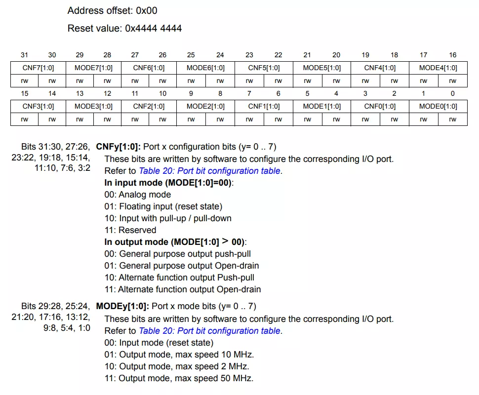
GPIO Port configuration register low (GPIOx_CRL)
This GPIO Port configuration register low (GPIOx_CRL) is used to select the I/O direction of pins 0 to 7.
|
|
|
GPIOx_CRL)GPIO Port configuration register high (GPIOx_CRH)
This GPIO Port configuration register high (GPIOx_CRH) is used to select the I/O direction of pins 8 to 15.
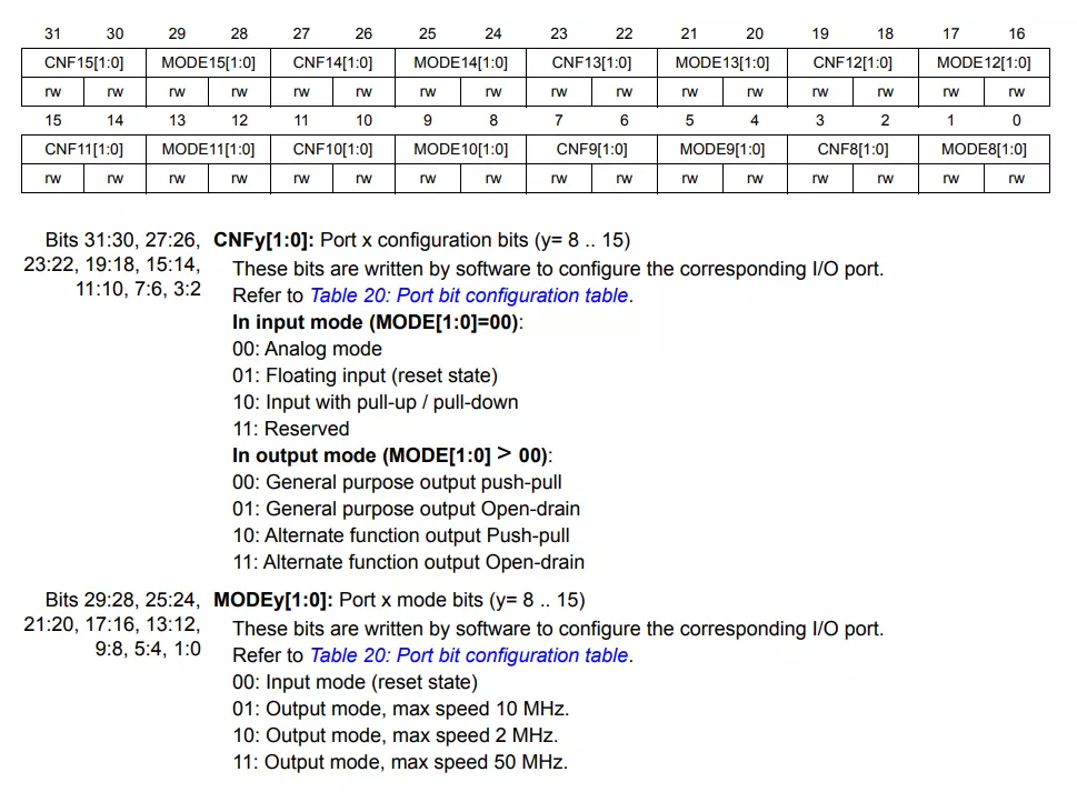
So, both CRL and CRH registers are used to set the GPIO direction.
Example:
In the below example, we are going to set PC13 and PC0 as output.
/* PC13 as output */
  GPIOC->CRH &= ~(GPIO_CRH_MODE13|GPIO_CRH_CNF13);    /* Clear MODE13 and CNF13 fields */
  GPIOC->CRH |= GPIO_CRH_MODE13_1|GPIO_CRH_MODE13_0;  /* Set MODE13 to 3 (Output) */

/* PC0 as output */
  GPIOC->CRL &= ~(GPIO_CRL_MODE0|GPIO_CRL_CNF0);    /* Clear MODE0 and CNF0 fields */
  GPIOC->CRL |= GPIO_CRL_MODE0_1|GPIO_CRL_MODE0_0;  /* Set MODE0 to 3 (Output) */
Data Registers
These data registers are used to store the data to be output/input. The below registers are used for output/input.
|
|
|
- GPIO Port input data register (
GPIOx_IDR) - GPIO Port output data register (
GPIOx_ODR) - GPIO Port bit set/reset register (
GPIOx_BSRR) - GPIO Port bit reset register (
GPIOx_BRR)
GPIO Port input data register (GPIOx_IDR)
This register is used to read the GPIO status.

Example:
Let’s assume that I have configured PORT B as input, using the GPIOB_CRL and GPIOB_CRH register. Now we can read the GPIO pins like below.
//Reading PB0 bit
if( ( GPIOB->IDR & 0x01) == 0 )
{
  //PORT B's 0th bit is 0
}
else
{
  //PORT B's 0th bit is 1
}
//Reading full PB
uint32_t value = GPIOB->IDR;
//Reading PB15
bool value = (( GPIOB->IDR >> 15 ) & 0x1);
GPIO Port output data register (GPIOx_ODR):
This is the Output Data Register. When you have configured the GPIO Port as output using GPIOx_CRL and GPIOx_CRH register, this register is used to set the value to the GPIO pin. We can read and write to the register. Please find the below image of the GPIOx_ODR register.
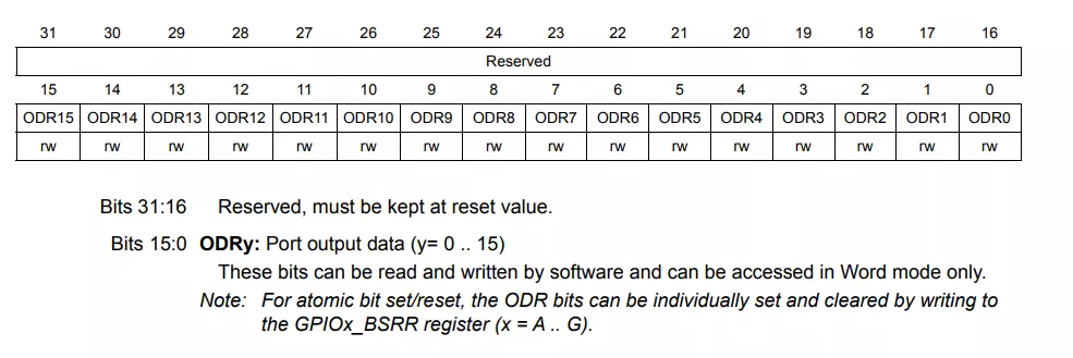
Example:
|
|
|
Let’s assume that I have configured PORT B as output, using the GPIOB_CRL and GPIOB_CRH register. Now we can write the GPIO pins like below.
//Write 1 to the full Port B
GPIOB->ODR = 0x0000FFFF;
//Write 0 to the full Port B
GPIOB->ODR = 0x00000000;
You have to be careful when you are writing the GPIO port using this GPIOx_ODR. Because you may disturb the other Pins (bits) of the register which you don’t want. Then what if I want to write a single bit without disturbing others? There is a way to do that. Just keep reading.
Port bit set/reset register (GPIOx_BSRR)
This is the GPIO Bit Set/Reset Register. When you want to set or reset a particular bit or pin, you can use this register. This is a write-only register. This register will do the atomic set/reset. So we don’t worry about the interrupts that cause problems during set/reset.
In this register, the lower 16 bits are used to set any of the 16 pins, and the higher 16 bits to clear/reset any of the 16 pins of a particular IO port. Please find the below image of the GPIOx_BSRR register.

Example:
|
|
|
Let’s assume that I have configured PORT B as output, using the GPIOB_CRL and GPIOB_CRH register. Now we can write the GPIO pins like below.
//set all the bits of Port B
GPIOB->BSRR = 0x0000FFFF;
//Clear all the bits of Port B
GPIOB->BSRR = 0xFFFF0000;
//Set the 5th bit of Port B
GPIOB->BSRR = (1U << 5);
//Clear the 5th bit of Port B
GPIOB->BSRR = (1U << 21);
Locking Registers
This register is used to lock the configuration of the port bits. The below register is used to do that.
- GPIO Lock register (
GPIOx_LCKR)
GPIO Port configuration lock register (GPIOx_LCKR)
This register is used to lock the configuration of the port bits when a correct write sequence is applied to bit 16 (LCKK). The value of bits [15:0] is used to lock the configuration of the GPIO. During the write sequence, the value LCKR[15:0] must not change.
When the LOCK sequence has been applied on a port bit it is no longer possible to modify the value of the port bit until the next reset. Each lock bit freezes the corresponding 4 bits of the control register (CRL, CRH).

Lock key write sequence:
As per the datasheet, below is the lock key write sequence.
|
|
|
Write 1
Write 0
Write 1
Read 0
Read 1 (this read is optional but confirms that the lock is active)
Note: During the Lock key write sequence, the value of LCK[15:0] should not change. And in some other STM32, this GPIOx_LCKR is not available for all the GPIO ports. So you should check with the datasheet before doing this. However, in the STM32F411CE, the GPIOx_LCKR register is available for all the GPIO ports.
Any error in the lock key write sequence aborts the lock. Once you have done the lock key write sequence properly on any bit of the port, any read access on the LCKK bit will return ‘1’ until the next CPU reset.
I think we have covered almost all the registers. Now we will just put them all together and make our hands dirty by playing with the LEDs. Let’s dive into the programming part.
STM32 GPIO Tutorial – LED Interfacing with STM32
You can refer to the respective User manual for a better understanding.
|
|
|
STM32F4 Code
In the below example, I am going to toggle the Onboard LED which is connected to the PC13. I have set the PC13 as an output. and toggling that with some delay. You can also find the complete project on GitHub.
Code:
/***************************************************************************//**
*   \file       main.c
*
*   \details    Blinking Onboard LED with some random delay - STM32 GPIO Tutorial
*
*   \author     EmbeTronicX
*
*   \This code is verified with STM32411CE Board
*
*******************************************************************************/

#include "stm32f4xx.h"

#define DELAY_COUNT    ( 80000 )   /* delay count */

/***************************************************************************//**

  \details  Providing Delay by running empty for loop

  \return   void

  \retval   none

*******************************************************************************/
static void delay( void )
{
    uint32_t i = 0;
    for( i=0; i<=DELAY_COUNT; i++ );
}

/***************************************************************************//**

  \details  The main function.  It should not return.

  \return   void

  \retval   none

*******************************************************************************/
int main(void)
{
  /* Enable the AHB clock all GPIO port C */
  SET_BIT(RCC->AHB1ENR, RCC_AHB1ENR_GPIOCEN);

  /* set all Port C as output */
  GPIOC->MODER = 0x55555555;

  /* Endless loop */
  while(1)
  {
    /* Turn ON the LED of PC13 */
    GPIOC->BSRR |= GPIO_BSRR_BS13;

    delay();

    /* Turn OFF the LED of PC13 */
    GPIOC->BSRR |= GPIO_BSRR_BR13;

    delay();
  }
}
STM32F1 Code
In the below example, I am going to toggle the Onboard LED which is connected to the PC13. I have set the PC13 as an output. and toggling that with some delay. You can also find the complete project on GitHub.
Code:
/***************************************************************************//**
*   \file       main.c
*
*   \details    Blinking Onboard LED with some random delay - STM32 GPIO Tutorial
*
*   \author     EmbeTronicX
*
*   \This code is verified with STM32F103CBT6 Board
*
*******************************************************************************/

#include "stm32f10x.h"

#define DELAY_COUNT    ( 80000 )   /* delay count */

/***************************************************************************//**

  \details  Providing Delay by running empty for loop

  \return   void

  \retval   none

*******************************************************************************/
static void delay( void )
{
    uint32_t i = 0;
    for( i=0; i<=DELAY_COUNT; i++ );
}

/***************************************************************************//**

  \details  The main function.  It should not return.

  \return   void

  \retval   none

*******************************************************************************/
int main(void)
{
  /* Enable the APB clock all GPIO port C */
  SET_BIT(RCC->APB2ENR, RCC_APB2ENR_IOPCEN);

  /* PC13 as output */
  GPIOC->CRH &= ~(GPIO_CRH_MODE13|GPIO_CRH_CNF13);    /* Clear MODE13 and CNF13 fields */
  GPIOC->CRH |= GPIO_CRH_MODE13_1|GPIO_CRH_MODE13_0;  /* Set MODE13 to 3 (Output) */

  /* Endless loop */
  while(1)
  {
    /* Turn ON the LED of PC13 */
    GPIOC->BSRR |= GPIO_BSRR_BS13;

    delay();

    /* Turn OFF the LED of PC13 */
    GPIOC->BSRR |= GPIO_BSRR_BR13;

    delay();
  }
}
STM32F7 Code
In the below example, I am going to toggle the Onboard LEDs which are connected to PB0 (Green LED), PB7 (Blue LED), and PB14 (Red LED). I have set the PB0, PB7, and PB14 as output, and toggling those with some delay. You can also find the complete project on GitHub.
Code:
/***************************************************************************//**
*   \file       main.c
*
*   \details    Blinking Onboard LED with some random delay - STM32 GPIO Tutorial
*
*   \author     EmbeTronicX
*
*   \This code is verified with STM32F767Zi Nucleo Board
*
*******************************************************************************/

#include "stm32f7xx.h"

#define DELAY_COUNT    ( 80000 )   /* delay count */

/***************************************************************************//**

  \details  Providing Delay by running empty for loop

  \return   void

  \retval   none

*******************************************************************************/
static void delay( void )
{
    uint32_t i = 0;
    for( i=0; i<=DELAY_COUNT; i++ );
}

/***************************************************************************//**

  \details  The main function. It should not return.

  \return   void

  \retval   none

*******************************************************************************/
int main(void)
{
  /* Enable the AHB clock all GPIO port B */
  SET_BIT(RCC->AHB1ENR, RCC_AHB1ENR_GPIOBEN);

  /* set Port B as output */
  GPIOB->MODER |= 0x55555555;

  /* Set Port B as Push Pull */
  GPIOB->OTYPER = 0x00000000;

  /* Set Low Speed */
  GPIOB->OSPEEDR = 0x00000000;

  /* Endless loop */
  while(1)
  {
    /* Turn ON the PB0 (Green LED), PB7 (Blue LED), PB14 (Red LED) */
    GPIOB->BSRR |= GPIO_BSRR_BS0 | GPIO_BSRR_BS7 | GPIO_BSRR_BS14;

    delay();

    /* Turn OFF the PB0 (Green LED), PB7 (Blue LED), PB14 (Red LED) */
    GPIOB->BSRR |= GPIO_BSRR_BR0 | GPIO_BSRR_BR7 | GPIO_BSRR_BR14;

    delay();
  }
}
Output – STM32 GPIO Bare Metal
Please find the output of the example below.
STM32 GPIO Tutorial – Switch/Button Interfacing with STM32
STM32F4 Code
I have connected the button to the PA0 (Port A.0) and the LED to the PC13. You can also find the project on GitHub.
|
|
|
Code:
/***************************************************************************//**
*   \file       main.c
*
*   \details    Setting Port A0 as input and PORT C13 as output.
*               When we press the Port A0, we will turn on the LED in
*               PC13 - STM32 GPIO Tutorial
*
*   \author     EmbeTronicX
*
*   \This code is verified with STM32411CE Board
*
*******************************************************************************/

#include "stm32f4xx.h"

/***************************************************************************//**

  \details  The main function.  It should not return.

  \return   void

  \retval   none

*******************************************************************************/
int main(void)
{
  /* Enable the AHB clock all GPIO Port C and Port A */
  SET_BIT(RCC->AHB1ENR, RCC_AHB1ENR_GPIOCEN);
  SET_BIT(RCC->AHB1ENR, RCC_AHB1ENR_GPIOAEN);

  /* set Port C13 as output */
  GPIOC->MODER &= ~( GPIO_MODER_MODER13 );    /* Clear MODER13 fields */
  GPIOC->MODER |=  ( GPIO_MODER_MODER13_0 );  /* Set MODER13 to 1 (Output) */

  /* set Port A0 as input */
  GPIOA->MODER &= ~( GPIO_MODER_MODER0 );    /* Clear MODER0 fields to 0 (input) */

  /* Enable Pullup on PA0 */
  GPIOA->PUPDR &= ~( GPIO_PUPDR_PUPDR0 );    /* Clear PUPDR0 fields (No Pullup, No Pull down) */
  GPIOA->PUPDR |=  GPIO_PUPDR_PUPDR0_0;      /* Set PUPDR0 fields to 0x01 (Pullup) */

  /* Endless loop */
  while(1)
  {
    /* Button is connected to PA0. So we need to check bit 0 of IDR register. */
    if( ( GPIOA->IDR & GPIO_IDR_ID0) == GPIO_IDR_ID0 )
    {
      /* Turn ON the LED of PC13 */
      GPIOC->BSRR |= GPIO_BSRR_BS13;
    }
    else
    {
      /* Turn OFF the LED of PC13 */
      GPIOC->BSRR |= GPIO_BSRR_BR13;
    }
  }
}
STM32F1 Code
I have connected the button to the PA0 (Port A.0) and the LED to the PC13. You can also find the project on GitHub.
Code:
/***************************************************************************//**
*   \file       main.c
*
*   \details    Setting Port A0 as input and PORT C13 as output.
*               When we press the Port A0, we will turn on the LED in
*               PC13 - STM32 GPIO Tutorial
*
*   \author     EmbeTronicX
*
*   \This code is verified with STM32F103CBT6 Board
*
*******************************************************************************/

#include "stm32f10x.h"

/***************************************************************************//**

  \details  The main function.  It should not return.

  \return   void

  \retval   none

*******************************************************************************/
int main(void)
{
  /* Enable the APB clock all GPIO Port C and Port A */
  SET_BIT(RCC->APB2ENR, RCC_APB2ENR_IOPCEN);
  SET_BIT(RCC->APB2ENR, RCC_APB2ENR_IOPAEN);

  /* PC13 as output */
  GPIOC->CRH &= ~(GPIO_CRH_MODE13|GPIO_CRH_CNF13);    /* Clear MODE13 and CNF13 fields */
  GPIOC->CRH |= GPIO_CRH_MODE13_1|GPIO_CRH_MODE13_0;  /* Set MODE13 to 3 (Output) */

  /* PA0 as input with pullup */
  GPIOA->CRL &= ~(GPIO_CRL_MODE0|GPIO_CRL_CNF0);     /* Clear MODE0 and CNF0 fields */
  GPIOA->CRL |= GPIO_CRL_CNF0_1;                     /* Set CNF0 to 10 (Input with pullup/pull down) */
  GPIOA->ODR |= GPIO_IDR_IDR0;                       /* pull-up PA0 */

  /* Endless loop */
  while(1)
  {
    /* Button is connected to PA0. So we need to check bit 0 of IDR register. */
    if( ( GPIOA->IDR & GPIO_IDR_IDR0 ) == GPIO_IDR_IDR0 )
    {
      /* Turn ON the LED of PC13 */
      GPIOC->BSRR |= GPIO_BSRR_BS13;
    }
    else
    {
      /* Turn OFF the LED of PC13 */
      GPIOC->BSRR |= GPIO_BSRR_BR13;
    }
  }
}
STM32F7 Code
I have connected the button to the PC13 (Port C.13) and LED to the PB0, PB7, and PB14. You can also find the project on GitHub.
Code:
/***************************************************************************//**
*   \file       main.c
*
*   \details    Setting Port B as output and PORT C13 as input.
*               When we press the Port C13, we will turn on the PB0, PB7, PB14 - STM32 GPIO Tutorial
*
*   \author     EmbeTronicX
*
*   \This code is verified with STM32F767Zi Nucleo Board
*
*******************************************************************************/

#include "stm32f7xx.h"

/***************************************************************************//**

  \details  The main function.  It should not return.

  \return   void

  \retval   none

*******************************************************************************/
int main(void)
{
  /* Enable the AHB clock all GPIO Port B and Port C */
  SET_BIT(RCC->AHB1ENR, RCC_AHB1ENR_GPIOBEN);
  SET_BIT(RCC->AHB1ENR, RCC_AHB1ENR_GPIOCEN);

  /* set Port B0, B7, B14 as output */
  GPIOB->MODER &= ~( GPIO_MODER_MODER0 |
                     GPIO_MODER_MODER7 |
                     GPIO_MODER_MODER14 );    /* Clear MODER0, MODER7, MODER14 fields */

  GPIOB->MODER |=  ( GPIO_MODER_MODER0_0 |
                     GPIO_MODER_MODER7_0 |
                     GPIO_MODER_MODER14_0 );  /* Set MODER0, MODER7, MODER14 to 1 (Output) */

  /* set Port C13 as input */
  GPIOC->MODER &= ~( GPIO_MODER_MODER13 );    /* Clear MODER13 fields to 0 (input) */

  /* Disable Pullup/Pulldown on PC13 */
  GPIOC->PUPDR &= ~( GPIO_PUPDR_PUPDR13 );    /* Clear PUPDR13 fields (No Pullup, No Pull down) */

  /* Set Port B as Push Pull */
  GPIOB->OTYPER = 0x00000000;

  /* Set Low Speed */
  GPIOB->OSPEEDR = 0x00000000;

  /* Endless loop */
  while(1)
  {
    /* Button is connected to PC13. So we need to check bit 13 of IDR register. */
    if( ( GPIOC->IDR & GPIO_IDR_ID13) == GPIO_IDR_ID13 )
    {
      /* Turn ON the PB0 (Green LED), PB7 (Blue LED), PB14 (Red LED) */
      GPIOB->BSRR |= GPIO_BSRR_BS0 | GPIO_BSRR_BS7 | GPIO_BSRR_BS14;
    }
    else
    {
      /* Turn OFF the PB0 (Green LED), PB7 (Blue LED), PB14 (Red LED) */
      GPIOB->BSRR |= GPIO_BSRR_BR0 | GPIO_BSRR_BR7 | GPIO_BSRR_BR14;
    }
  }
}
Output – STM32 GPIO Bare metal
Please find the output of the example below.
If you want to use RTOS in STM32, you can refer to the STM32 GPIO with the RTOS tutorial. In our next tutorial, we will see the STM32 Timers and their registers with examples.
|
|
|
Please read the other STM32 Tutorials.
You can also read the below tutorials.

Embedded Software | Firmware | Linux Devic Deriver | RTOS
Hi, I am a tech blogger and an Embedded Engineer. I am always eager to learn and explore tech-related concepts. And also, I wanted to share my knowledge with everyone in a more straightforward way with easy practical examples. I strongly believe that learning by doing is more powerful than just learning by reading. I love to do experiments. If you want to help or support me on my journey, consider sharing my articles, or Buy me a Coffee! Thank you for reading my blog! Happy learning!

